You are currently viewing SemiWiki as a guest which gives you limited access to the site. To view blog comments and experience other SemiWiki features you must be a registered member. Registration is fast, simple, and absolutely free so please,
join our community today!
Even though design management systems are gaining popularity as a way to manage design data growth, they actually contribute to the problem of exploding data size. What we already know is that a linear increase in die size causes exponential growth in chip area, and that smaller feature sizes compound this effect in the same way.… Read More
The topic of Product Lifecycle Management (PLM) conjures up images of usage on airplanes, tanks and cars. That’s because it was developed decades ago to help make product development and delivery more efficient for big expensive manufactured products. It worked well for its intended markets by combining and managing all the … Read More
Whether or not in the past you believed all the of rhetoric about exploding design complexity in SOC’s, today there can be no debate that SOC size and complexity is well beyond something that can be managed without some kind of design management system. As would be expected, development of most larger designs relies on a data management… Read More
How can large SOC projects effectively integrate sub blocks and IP into a stable version for release or internal development? The person responsible for integrating SOC sub blocks into a validated configuration for release has a difficult task. Usually there are many sub-blocks, each undergoing their own development. There… Read More
Is a software development release methodology a “square peg in a round hole” when it comes to hardware design? To answer this question we have to look at how exactly hardware design projects differ from their software counterparts. Intuitively we know they are fundamentally different. Let’s take a second to dig deeper to understand… Read More
Years ago I thought that chip design companies would embrace the latest technology and be eager to adopt new tools. What I learned was that the people implementing and managing design projects were taking a lot of risks with almost every aspect of their projects. What they most wanted is to minimize risk from the design process – especially… Read More
Best practices call for using a version control system with systematic releases when developing IP. However, in the early stages of IP development using a rigid version control system with a cumbersome release process can hinder productivity. To fully understand how this works we should start by defining what is meant when we … Read More
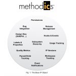
When the term IP first came into popular usage for IC design, it was primarily conceived as blocks of design content that were bought occasionally from external sources. A customer might use one or two in a design, and expect one delivery with perhaps some minor updates before tapeout. Over the last 18 years, this notion has changed… Read More
Let’s just take it as a given that securing IP design data is critical. It’s rather like saying that it’s a good idea to have security in the Tower of London to stop the crown jewels being stolen. IP blocks are the crown jewels of an SoC company.
Data now must be secured within the collaborative teams that share that… Read More
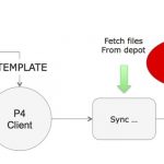
Almost all large projects these days are distributed across multiple geographic locations. As the world rotates underneath the sun, the focus of activity moves too: Europe, US, China, India, back to Europe. For this to work effectively requires a collaborative platform designed for multi-site design efforts, a platform that… Read More