You are currently viewing SemiWiki as a guest which gives you limited access to the site. To view blog comments and experience other SemiWiki features you must be a registered member. Registration is fast, simple, and absolutely free so please,
join our community today!
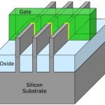
In the semiconductor industry, it feels great to hear about the process technology shrinking to lower nodes along with innovative transistor structures that offer major gains in PPA (Power, Performance and Area). However, it requires huge investment of capital, time and effort from foundries to conceptualize, prototype and… Read More
Ever since I have seen Atrenta’s SpyGlass platform providing a comprehensive set of tools across the semiconductor design paradigm, I felt the need for a common set of standards to evolve for sign-off at RTL level. Last December, when I read an EE Times articleof Piyush Sancheti, VP, Product Marketing at Atrenta, where he talks … Read More