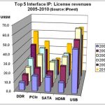
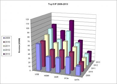
Is it surprising to see that Synopsys has been selected Interface IP partner of the year by TSMC? Not really, as the company is the clear leader on this IP market segment (which includes USB, PCI Express, SATA, DDRn, HDMI, MIPI and others protocols like Ethernet, DisplayPort, Hyper Transport, Infiniband, Serial RapidIO…). But,… Read More
Tag: ddr4
Cadence Verification IP Technical Seminar!
According to trusted sources it costs upwards of $50M to design a 40nm SoC down to the GDS. Semiconductor IP is a fast growing part of that equation and functional verification of that IP is critical. Hardware complexity growth continues to follow Moore’s Law but verification complexity is even more challenging. In fact, IP verification… Read More
Cadence VIP Seminar: next stop after Denali party, August 25th in San Jose
If you did not have the chance to attend the famous Denali party at DAC 2011, you may want to go to Cadence VIP seminar to be held on Thursday, August 25, 2011, from 1:00 – 4:15pm at Cadence Headquarters: 2655 Seely Avenue, San Jose, Building 10. To register, click here. The atmosphere could be slightly different, as during Denali… Read More
DDR4 Controller IP, Cadence IP strategy… and Synopsys
I will share with you some strategic information released by Cadence last week about their IP strategy, more specifically about the launch of the DDR4 Controller IP. And try to understand Cadence strategy about Interface IP in general (USB, PCIe, SATA, DDRn, HDMI, MIPI…) and how Cadence is positioned in respect with their closest… Read More


