You are currently viewing SemiWiki as a guest which gives you limited access to the site. To view blog comments and experience other SemiWiki features you must be a registered member. Registration is fast, simple, and absolutely free so please,
join our community today!
As analog and mixed-signal designs become increasingly complex, parasitic effects dominate both design time and cost, consuming 30–50% of engineers’ effort in debugging and reanalyzing circuits. Addressing these multiphysics effects requires early verification strategies and reliable simulation solutions. Modern … Read More
Often when a company starts out it takes a while for it to find the sweet spot in the marketplace. Very often it is feedback from existing customers and business success that can help point the way for small companies as they grow. This is just as true in EDA as it is in retailing or consumer products. For instance, Mentor Graphics, though… Read More
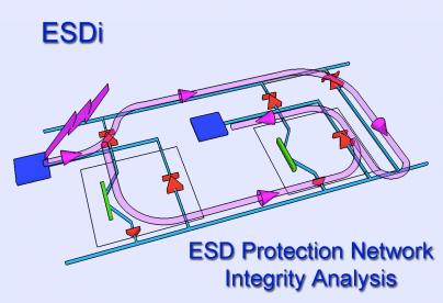
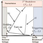
I’ve written before about anti-fuse non-volatile memory, where the gate oxide is intentionally damaged in order to create a readable bit of data, but this is what most circuit designers never want to have happen to their logic gates. However, since the advent of MOS transistors the issue of Electrostatic Discharge (ESD) and the… Read More
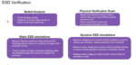
As Moore’s law keeps going, semiconductor design density on a chip keeps increasing. The real concern today is that the shrinkage in technology node has rendered the small wire geometry and gate oxide thickness (although fine in all other perspectives) extremely vulnerable to ESD (Electrostatic Discharge) effects. More than… Read More