Synopsys is catalyzing the era of pervasive intelligence with comprehensive engineering solutions spanning silicon design, IP, and simulation and analysis. At this year’s Design Automation Conference (DAC), the company will showcase innovations transforming silicon and systems development for a wide range of applications… Read More
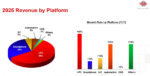
The semiconductor landscape is currently undergoing a structural transformation as the “Data-Centric Shift” moves the industry’s center of gravity from smartphones toward High-Performance Computing (HPC) and AI infrastructure.
This transition is clearly validated by TSMC’s 2025 filings, which show… Read More
CadenceLIVE Indiaby Admin on 06-16-2026 at 1:46 pm
Join us on August 12 for CadenceLIVE India 2026, where Cadence technology users connect with the engineers and industry leaders who develop the solutions and the industry experts who influence market trends.
Participants experience a day of learning, connection, and cutting-edge technology shaping the future of electronic… Read More
“How Will Agentic AI Change Chip Design and Verification?” features EDA and emerging agentic AI company executives and entrepreneurs discussing changes within chip design and verification as agentic AI tools become more mainstream. Panelists will distill the excitement surrounding the innovation in chip design and verification,… Read More
Join us at CadenceCONNECT: Tech Days Europe 2026, our annual, free, multi-track event dedicated to the engineers, innovators, and visionaries shaping the future of electronic design. Our aim is to bring together like minded thinkers to explore how AI-driven Cadence technologies are transforming design workflows, boosting… Read More
Join us at CadenceCONNECT: Tech Days Europe 2026, our annual, free, multi-track event dedicated to the engineers, innovators, and visionaries shaping the future of electronic design. Our aim is to bring together like minded thinkers to explore how AI-driven Cadence technologies are transforming design workflows, boosting… Read More
Join us at CadenceCONNECT: Tech Days Europe 2026, our annual, free, multi-track event dedicated to the engineers, innovators, and visionaries shaping the future of electronic design. Our aim is to bring together like minded thinkers to explore how AI-driven Cadence technologies are transforming design workflows, boosting… Read More
Join us at CadenceCONNECT: Tech Days Europe 2026, our annual, free, multi-track event dedicated to the engineers, innovators, and visionaries shaping the future of electronic design. Our aim is to bring together like minded thinkers to explore how AI-driven Cadence technologies are transforming design workflows, boosting… Read More
Join us at CadenceCONNECT: Tech Days Europe 2026, our annual, free, multi-track event dedicated to the engineers, innovators, and visionaries shaping the future of electronic design. Our aim is to bring together like minded thinkers to explore how AI-driven Cadence technologies are transforming design workflows, boosting… Read More
Join us at CadenceCONNECT: Tech Days Europe 2026, our annual, free, multi-track event dedicated to the engineers, innovators, and visionaries shaping the future of electronic design. Our aim is to bring together like minded thinkers to explore how AI-driven Cadence technologies are transforming design workflows, boosting… Read More