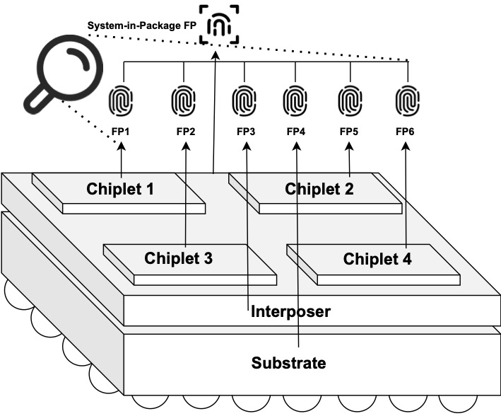
In the quest to secure the authenticity and ownership of advanced integrated circuit (IC) packages, a novel approach has been introduced in this paper that capitalizes on the inherent physical discrepancies within these components. This method, distinct from traditional strategies like physical unclonable functions (PUFs) and cryptographic techniques, harnesses the unique defect patterns naturally occurring during the manufacturing process. Counterfeiting involves unlawfully replicating authentic items for unauthorized advantages or financial gain, affecting diverse sectors such as automotive components, electronics, and consumer goods. Counterfeit integrated circuits (ICs) if sold in open market present a substantial risk due to their deviations in functionality, material composition, and overall specifications.
These illegitimate micro-electronic products, which might be mislabeled, reused, or cloned, fall into two primary categories: those with functional differences (like incorrect labeling or false specifications) and those that mimic the original function yet differ in technical aspects such as circuit timing or stress tolerance. Incorporating such counterfeit ICs into electronic devices can lead to significant adverse effects, undermining the devices’ quality, reliability, and performance. The stakes are especially high in military contexts, where the reliability and security of electronic systems are of paramount importance. According to a report from the International Chamber of Commerce , counterfeit trading globally is valued at up to 1 trillion USD each year, with the electronics sector making up a substantial share of this market.
The rise in counterfeit ICs has been linked to practices like outsourcing production to untrusted entities or due to the absence of proper life cycle management or traceability framework. Detection of counterfeits is perceived to be a more viable approach than prevention. Prevention requires extensive collaboration across borders, industries, and legal frameworks. Given the global nature of supply chains and the sophistication of counterfeit operations, prevention efforts can be difficult to implement and enforce consistently. However, the approach of detection offers flexibility, cost-effectiveness, and the ability to adapt to the changing tactics of counterfeiters. Despite extensive research into methods for detecting counterfeit ICs over the past decade, differentiating between new and used ICs, as well as spotting illegally produced or altered ICs, continues to be a significant challenge.
The introduction of sophisticated multi-die packaging technologies further complicates the issue of counterfeiting. These technologies which combine multiple chiplets into a single package increases the likelihood of counterfeit components being introduced into the system. The complexity of these systems where chiplets from various sources are integrated into one package, makes verifying the authenticity of each component more challenging, raising the potential for counterfeit chiplets to affect the system’s overall functionality and security.

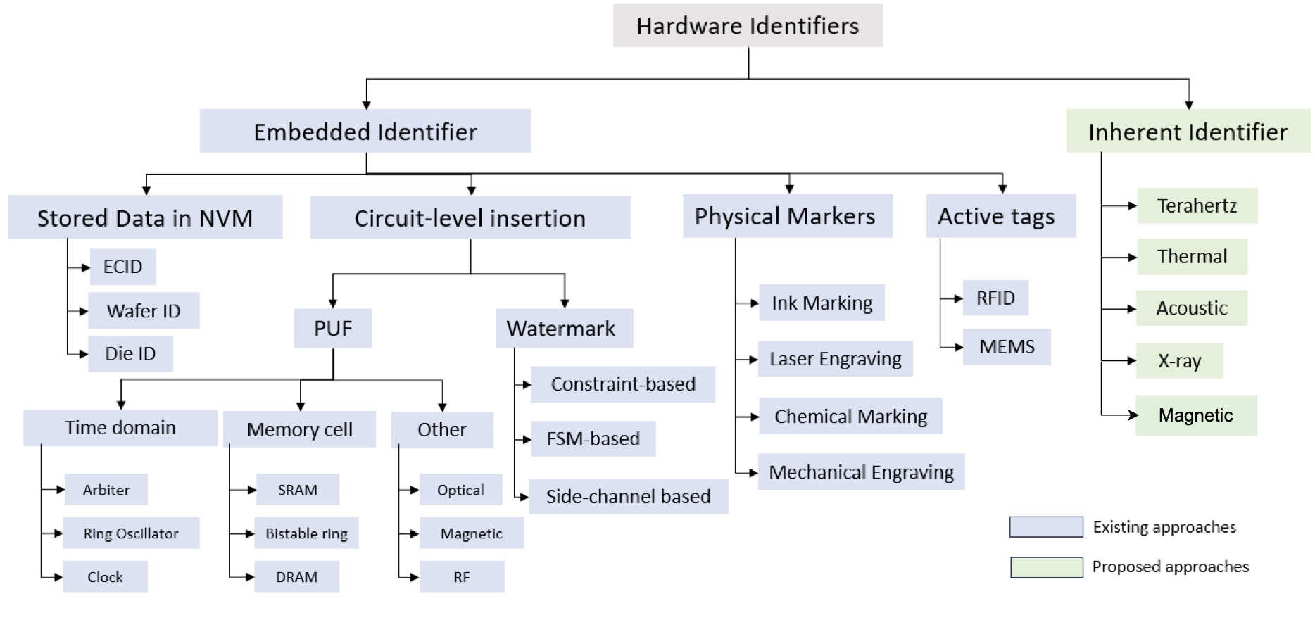
This new landscape of IC packaging necessitates a new direction for enabling reliable provenance. Provenance allows for the authentication of components at any stage of the supply chain. Buyers can verify whether an IC matches its documented history, ensuring its authenticity which reduces the risk of counterfeit ICs being accepted and used in critical systems. Provenance requires a method of identification in the die level, package level or board level. Historically, this is achieved by embedding some form of hardware identifier into the IC. These identifiers can be as simple as placing physical markers on the IC package or the die or storing manufacturing data in a non-volatile memory inside the chip or inserting additional circuitry to serve as an electrical watermark which makes it possible to trace the batch or wafer number of origin of a particular IC.
Hardware fingerprinting has emerged as a potent method for achieving provenance in the fight against counterfeit electronics. For example, physical unclonable functions (PUF) leverages the unique, manufacturing process variation of hardware components to provide a means of identifying and authenticating genuine devices throughout their lifecycle. However, despite being in spotlight for more than two decades, PUF based fingerprinting is yet to be widely adopted in industry. This can be attributed to a number of reasons including sensitivity to environmental conditions, risk of physical degradation over time, scalability and integration challenges within manufacturing processes, challenges in enrollment and response provisioning, high resource demands for error correction, susceptibility to advanced security attacks, reliability concerns across the device’s lifespan, and issues with standardization and interoperability.
In this work, the authors visit the existing challenges and limitations of traditional embedded fingerprinting and watermarking approaches and propose the notion of inherent hardware identifiers using Thermo-reflectance Imaging (TRI) as a new frontier of opportunity for effective security assurance of advanced IC packaging supply chain as categorized in Figure 2.

The key contributions of this work are summarized as follows: 1. Review existing embedded fingerprinting and watermarking. 2.Highlight the limitations and challenges of the existing approaches when applied in the context of security of chiplets and multi-chiplet systems or SiP. 3.Introduce the concept of inherent identifiers for fingerprinting and watermarking.4. Demonstrate TRI to harness inherent uniqueness to create fingerprints and watermarks.
Navid Asadizanjani
Associate Professor, Alan Hastings Faculty Fellow, Director, Security and Assurance lab (virtual walk), Associate director, FSI, MEST, Department of Electrical and Computer Engineering, Department of Material Science and Engineering, University of Florida
Nitin Vershney
Research Engineer, Florida Institute for Cybersecurity Research
Also Read:
Navigating Frontier Technology Trends in 2024
PQShield Builds the First-Ever Post-Quantum Cryptography Chip
Share this post via:


Chemical Origins of Environmental Modifications to MOR Lithographic Chemistry