Back in June 2021, Patently Apple posted a report titled " TSMC's 3DFabric Technology is the next big wave in Chip Design that Apple will take advantage of in the not-too-distant Future." The report noted TSMC's CEO CC Wei stating, "We observe chiplets are becoming an industry trend. We are working with several customers on 3DFabric to enable chiplet architecture.
Today we're learning that Apple supplier Taiwan Semiconductor Manufacturing Co. (TSMC) is exploring a new method of advanced chip packing as the world's biggest chipmaker races to keep pace with the AI-fueled demand for computing power.
According to a new report by Nikkei Asia, " The idea behind the new approach is to use rectangular panel-like substrates, rather than the conventional round wafers used today, allowing more sets of chips to be placed on each wafer.
The study is still in its early stages, but it represents a significant technical shift by TSMC, which previously viewed the use of rectangular substrates as too challenging. To make the new method work, TSMC and its suppliers would have to devote a significant amount of time and effort to development as well as upgrade or replace numerous production tools and materials.
The rectangular substrate currently in trials measures 510 millimeters by 515 millimeters and has a usable area more than three times bigger than that of round wafers, sources briefed on the matter said. The rectangular shape means there would also be less unused area left over at the edges, sources said.
TSMC's advanced chip stacking and assembly techniques -- used to produce AI chips for the likes of Nvidia, AMD and others. 2-inch silicon wafers, The chipmaker is expanding its advanced chip packaging capacity in Taiwan to keep up with runaway demand. The expansion in Taichung is mainly for Nvidia, sources briefed on the matter said.
Chip packaging technology, once viewed as a relatively low-tech aspect of chipmaking, has become increasingly important to maintaining the pace of semiconductor advancement.
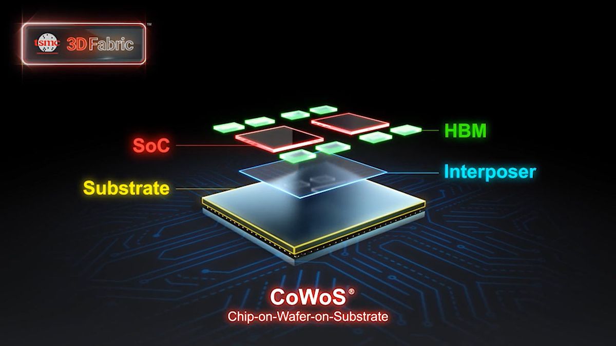
For AI computing chips like Nvidia's H200 and B200, using state-of-the-art chip production alone is not enough. Advanced chip packaging technology called CoWoS, chip-on-wafer-on-substrate pioneered by TSMC, is also necessary. For B200 chipsets, for example, CoWoS makes it possible to combine two Blackwell graphic processing units and connect them with eight high bandwidth memories (HBMs), enabling fast data throughput and accelerated computing performance.
But as chip size grows to accommodate more transistors and to integrate more memory, the current industry standard -- 12-inch wafers with an area of approximately 70,685 sq. millimeters -- may not be efficient enough for packaging cutting-edge chips in a couple of years.
For example, only 16 sets of the B200 can be built on a single wafer, and that is assuming the production yield is 100%, according to chip industry executives. About 29 sets of the earlier H200 and H100 chips can be packaged on one wafer, according to an estimate by Morgan Stanley.
'The trend is certain. The size of the package will only grow bigger [as chipmakers] squeeze more computing power out of chips used for AI data center computing,' one chip executive told Nikkei Asia. "But this is still at an early stage. For example, the coating of photoresists in cutting-edge chip packaging on a new shape of substrate is one of the bottlenecks. It takes the deep pockets of chipmakers like TSMC to push equipment makers to change equipment designs."
Display and PCB makers are specialists when it comes to handling rectangular substrates, but chip production demands a higher level of equipment and material precision, industry executives and analysts said.
Mark Li, a semiconductor analyst with Bernstein Research, said TSMC may need to consider using rectangular substrates soon because AI chipsets are going to require ever more chips per package.
While the shift is a certainty, TSMC continues to work with equipment and material suppliers on the new method that could take a few years before it's commercialized.
AI is a disruptive technology and TSMC is pushing the envelope in packaging chips to take all manor of computers to the next-level.