Array
(
    [content] => 
    [params] => Array
        (
            [0] => /forum/threads/tsm-builds-capacity-on-orders-only-others-should-take-note.18364/page-2
        )

    [addOns] => Array
        (
            [DL6/MLTP] => 13
            [Hampel/TimeZoneDebug] => 1000070
            [SV/ChangePostDate] => 2010200
            [SemiWiki/Newsletter] => 1000010
            [SemiWiki/WPMenu] => 1000010
            [SemiWiki/XPressExtend] => 1000010
            [ThemeHouse/XLink] => 1000970
            [ThemeHouse/XPress] => 1010570
            [XF] => 2021770
            [XFI] => 1050270
        )

    [wordpress] => /var/www/html
)

TSM builds capacity on orders only, Others should take note

I’ve been trying to understand how all the investments at the logic big three make sense. Basically to answer the “why now, what changed”.

One thing I didn’t realize is the average auto price has doubled in the last few years. It’s now $50K. And there isn’t really anything for less than that. The high price of cars really supports semiconductor supply chain.

The other thing is Apple‘s Macintosh desktop PC line. The M2 Studio is out, and getting reasonable reviews, for $4-5K each, equipped. The AR glasses are $3.5K. That really supports the desktop Mac market.

My argument is, pricing power from big end markets, from AI to desktop Macs, to autos, basically doubling prices, allows fabs to build new capacity to supply the market, and perhaps oversupply it, but without brutal competition, since there is so much fat on this animal.
 
For chips that is how you calculate performance. I'm talking from a process perspective. 22nm is listed as 18% more performant than 32nm. For top desktop parts clockspeed of sandy->ivy went up 100MHz. Sky-> kaby single core turo was only a 20% boost rather than the 26% performance from 14++. Did intel lie? No. This is just the post Dennard world we live in where you don't get power and density and clocks for no work. At the low end of the voltage curve where the leakage is manageable you will see performance = clockspeed. But at high voltages not so much.

Because if at x voltage you clock y% faster you can lower voltage and get the same performance. If iso power is acceptable you can keep voltage the same and get enough performance to potentially make up for a density disadvantage.

This is my whole point. A hypothetical 18A HPC chip should use less power at iso performance to an N2 chip. If you want to use the extra density N2 provides to add more SMs/EUs/CUs, you can do that @iso die are, but you will be adding that to your power budget (even if it is generally more efficient than boosting freq).

That is my bad, I misunderstood your wording.

Technically 18A is the only IFS node with no locked in customer deal at this point. Presumably if there was we would have heard it during an investor call. Timing has everything to do with a node's competitiveness. If I am a first wave TSMC customer intel 3 has no value to me, because N3E is coming out with close enough PPW and better density. If I am a second wave customer intel 3 is also dead to me because it is only going to start it's deprecation/yield/cost learning curves with the intel 4 ramp (leading to higher wafer pricing than what TSMC will probably offer from their soon to be fully depreciated N5 fabs). If intel 3 came out in 2021 they would be far enough along the listed curves that they could snag more second wave customers, and snag wave 1 customers from the WAY better performance and power characteristics. Density would also not be a problem given HP library is pretty darn close to the N5 HD.

I don't think you understand intel 4/3. For one density is not a feature it is a characteristic. By this notion intel 7 and N5 are not fully featured because they are less dense than N3E (which would also be missing features compared to N2). Two as far as we know, intel 4 only has a HP library and the devices to allow the MTL CPU die to talk with everything else. As far as we can tell from VLSI, intel 4 can make no other products besides MTL and the "custom networking ASIC".

Having all of the devices to make a fully featured SOC (supporting a radio being optional) is a good start.

I can see the slightly misleading angle to it. Truth be told if I was CEO for a day when this was made, I would have moved away from any scheme that could be implied to have a nm number or be compared to another firm's. I would have picked giving it some name, just calling it by the Pxxxx number, or use greek letters with numbers denoting nodelets in the series. I'm sure intel's argument would probably be that intel's metric since the day of intel accelerated has ALWAYS been "process performance per watt leadership by 2025". If that is the metric we are measuring, then I suppose you could even call it intel 2. Although I (and many many others) would not take kindly to this name. I suspect the 4/3 names were chosen by the following logic:

"Our HP library has the same density as N5's HD and we have better PPA/PPW than N5-N4P but worse density than N3. Let's call our node intel 4 as it sits kind of between them.".
Someone then asked "What do we call our 18% performance kicker once we enable the rest of the PDK?".
The response was "We don't want to do +s any more given how we ran that into the ground. 18% is also a full node on the PPW front and TSMC has lowered the number by doing less, all right we'll call it intel 3".

As for the nm number I am not going down this rabbit hole. The numbers stopped corresponding to features since like 130nm. Since then they only communicate that things are advancing.
I'm not sure we're disagreeing on that much.

Intel uses terms that aren't 100% accurate, not because they are lying, but because they have to oversimplify it to the point it is meaningful. If they said it's 18% more clock speed at point A, 15% more efficient at point B, etc..., it would get a message across.

Intel has not announced an 18a customer, but they have said there are important customers they will be announcing. But, sadly, I kind of remember similar talk around Intel 3, but with a little less conviction. But, that's just my interpretation. I think Intel has clearly lost I3/3nm, and that's a big one to lose, since it's the last FinFET. I have a pretty big investment in Intel, and it doesn't make me happy.

If you want to present having everything I4 lacks, as being able to make a broad spectrum of products, rather than a narrow one, no disagreement. It was just a bit nebulous to me without that qualification. But, that's not everything they need to sell it in a meaningful way, at least I don't think so.

I COMPLETELY agree with you on the naming. It's meaningless as a reference to size, and has been, so why keep using it? And if we consider processors, they (well AMD led the way with the K5), have moved away from clock speed as a naming convention a long time ago. Clock speed is still a real parameter too! And a pretty important one.

Now, if you can tell me that I3 having roughly half the density of TSMC's 3nm is something you anticipated, good for you, because I have to say I'm quite disappointed with it, and did not anticipate that much of a delta. 18A doesn't worry me so much, it's reasonable given the performance, and it also makes sense given how much importance Intel puts on clock speed. At 78% of the density (reversed), it's not terribly damning, especially given the performance. But, I3 at 48% (reversed) just seems problematic, especially given that Intel has indicated its cost structure will be higher. So, who needs the extra performance? GPUs? Not really, they'll like the density better, and we don't know where this performance advantage really kicks in the "powerband", if you will. Most ARM applications are not relying on performance at the wattages this would likely be advantageous at. And that's the part we were talking about. Do we really think this "performance" delta exists in phone scenarios? Or even ARM servers? It's not clear to me. It's my guess the author was talking about primarily top clock speed at relatively higher power usages, which don't necessarily approximate a broad range of usage scenarios. But, surely, some will see a benefit.

But, I think we both agree the one data point we're missing is power usage. That could change a whole lot of how we look at things. If Intel can deliver really good power characteristics in a broad spectrum of usage scenarios, I think it can still be an attractive node for a decent amount of potential customers. But, without that data, I have to admit, I'm a little disappointed with I3. But, 18A? I'd hate to be AMD trying to compete with that :p. Then again, even I3 should give Intel a nice boost for their internal designs.
 
I’ve been trying to understand how all the investments at the logic big three make sense. Basically to answer the “why now, what changed”.

One thing I didn’t realize is the average auto price has doubled in the last few years. It’s now $50K. And there isn’t really anything for less than that. The high price of cars really supports semiconductor supply chain.

The other thing is Apple‘s Macintosh desktop PC line. The M2 Studio is out, and getting reasonable reviews, for $4-5K each, equipped. The AR glasses are $3.5K. That really supports the desktop Mac market.

My argument is, pricing power from big end markets, from AI to desktop Macs, to autos, basically doubling prices, allows fabs to build new capacity to supply the market, and perhaps oversupply it, but without brutal competition, since there is so much fat on this animal.

I think for Intel, it's clear because they want to allow outside companies to use their fabs in a more substantial way than ever before. You have to be able to show you have the capacity for them.

For TSMC, you have such a dominant hold on the market, and given how many more types of products use semiconductors, or are using more of them, you feel confident that extra capacity will be needed. With all these silly devices needing more and more chips, and that list growing every day, I can kind of see their argument. And once people get used to being lazy slobs that have smart vacuum cleaners, there's no going back.

Samsung??? Does anyone ever know why Samsung does what they do? They seem to have a pretty strong disconnect with reality. It's amazing to me they haven't gone into researching semiconductor infused donkeys, while insisting they'll corner that potentially lucrative market. To their credit, they refuse to admit they suck. To their discredit, they do.
True. I can at least see the logic behind Intel's moves as of late. As for Samsung I have zero clue what they are doing or planning to do. I'm not sure they do either. Confidence is hardly inspired in leadership that a has a revolving door through the Korean legal system.
 
True. I can at least see the logic behind Intel's moves as of late. As for Samsung I have zero clue what they are doing or planning to do. I'm not sure they do either. Confidence is hardly inspired in leadership that a has a revolving door through the Korean legal system.

There has been change in Samsung leadership but the mission has always been to beat TSMC. Unfortunately, as the chart suggests, Samsung has always been behind TSMC in regards to implementation. Samsung 14nm was the exception as they split the Apple business on the iPhone 6. That was a painful decision for Apple as they do not like Samsung. Nor does Apple like Intel so any rumor of Apple switching is nonsense. Apple is dedicated to the pure-play foundry business, absolutely.

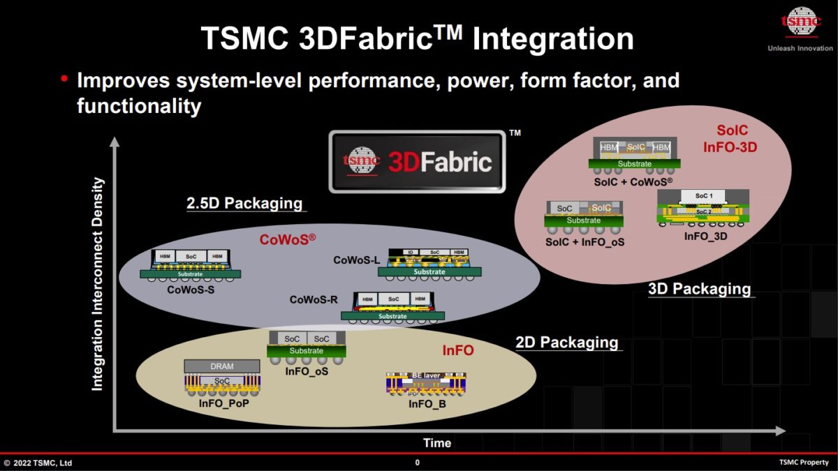
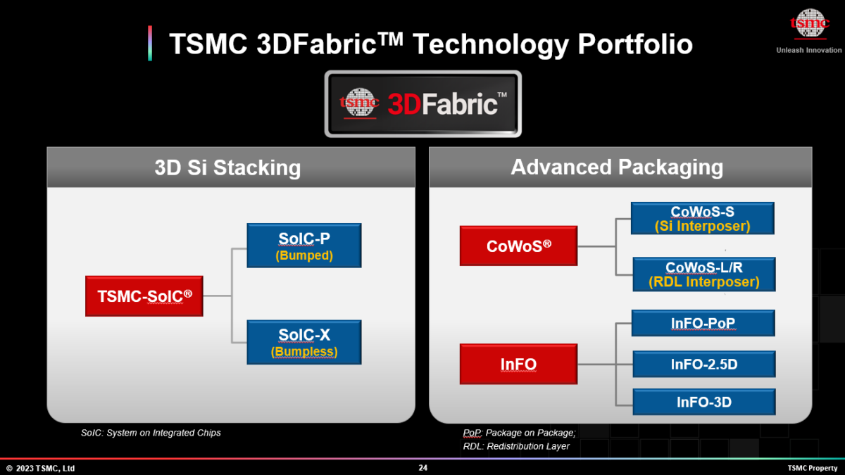
Packaging is now a game changer in the foundry business. IDM foundries certainly have the advantage since they have been packaging chips since the beginning of time. TSMC has the advantage of working closely with the top customers on packaging starting fresh. I would expect TSMC to continue to invest in packaging in an effort to keep the IDM foundries at bay.


We will be writing more about Intel and Samsung packaging shortly.
 
Just catching up with this thread, so apologies if I missed this answer somewhere.

Is there any meaningful normalised power comparison between these processes (referring back to the original normalised density and performance graphs) ? I've been hardwired into a PPA (power, performance, area) mindset. Not obvious you can extrapolate power from this data (and there may be process and library variants), though it tends to suggest TSMC 2nm would be lower.
Like performance, finding a hard number for power is not possible. However, the two are both two sides of the same coin. Based on the performance numbers you would expect 18A to do better in this regard. However exact power draw at any given voltage also depends on the on-leakage, off-leakage, Vmin, power loss from the interconnect stack, etc. Considering TSMC has more experience with lower power optimization, history would suggest that N2 has lower power draw near Vmin in spite of any "performance per watt advantage" intel might have. Additionally when one considers that this projection has N2's BSPDless HD lib denser than 18A's HD lib, you would expect N2 to have smaller devices. Smaller devices should result in higher off-leakage (all else being equal). 18A's larger nanosheet stack should allow for narrower sheets @iso drive current. BSPD should also result in lower power losses. To say nothing of other factors that impact power draw that hadn't occurred to me.

Long story short power is a very complex concept that we would need to see various different kind of applications to see how these node's PP characteristics compare across a wide variety of scenarios/configuration.
 
Last edited:
Single-threaded performance always is, although to varying degrees. If you need more cores to get the same performance, in the absolutely best case scenario, then you have an inferior processor. Because my cores will always be able to take advantage of their extra performance, whereas you'd need something that somehow could be able to use all the cores to equal the performance, and that's just not common for CPUs. GPUs? Yeah. For CPUs, you run into Amdahl's law.
We can break this down into markets. First, GPUs, where the $1.1T Nvidia shows the importance. Yeah, highly parallel. Also needs a lot of SRAM. Also needs - heck it needs everything. A hero in every aspect, from network to memory, and so hugely parallel they can make an 800mm2 chip yield by just ignoring the failing elements. Oh, and it would be really nice if it could avoid melting.

CPUs in servers. Lots of cores. Half or more of the area is SRAM. Easy to find parallel loads - different customers, plus mature apps like database or optimisation or web services that are multi-threaded. Proven cost savings due to more efficient packaging, lower power, shared resources, etc. with multiple cores. Hundreds of cores per package for sure. Again, avoid melting.

Mobile. Actually these have just a modest amount of cores. Half or more of the area is SRAM, then most of what is left is accelerations ranging from radio to graphics to inferencing to sensor fusion. More transistors welcome.

You can repeat the analysis for other markets. My point is that for the big markets we long since moved past Amdahl. His math is still valid, but we found multiple independent workloads and some very parallel specific workloads, so it is not the limiting factor.

If there is a universal pain point is is SRAM density, not Amdahl.
 
Back
Top