Samsung and Intel believe this is their best chance to close the game with TSMC
The world’s leading semiconductor companies are racing to make so-called “2 nanometer” processor chips that will power the next generation of smartphones, data centers, and artificial intelligence.Taiwan Semiconductor Manufacturing Company remains the analysts’ favorite to maintain its global supremacy in the sector, but Samsung Electronics and Intel have identified the industry’s next leap forward as a chance to close the gap.
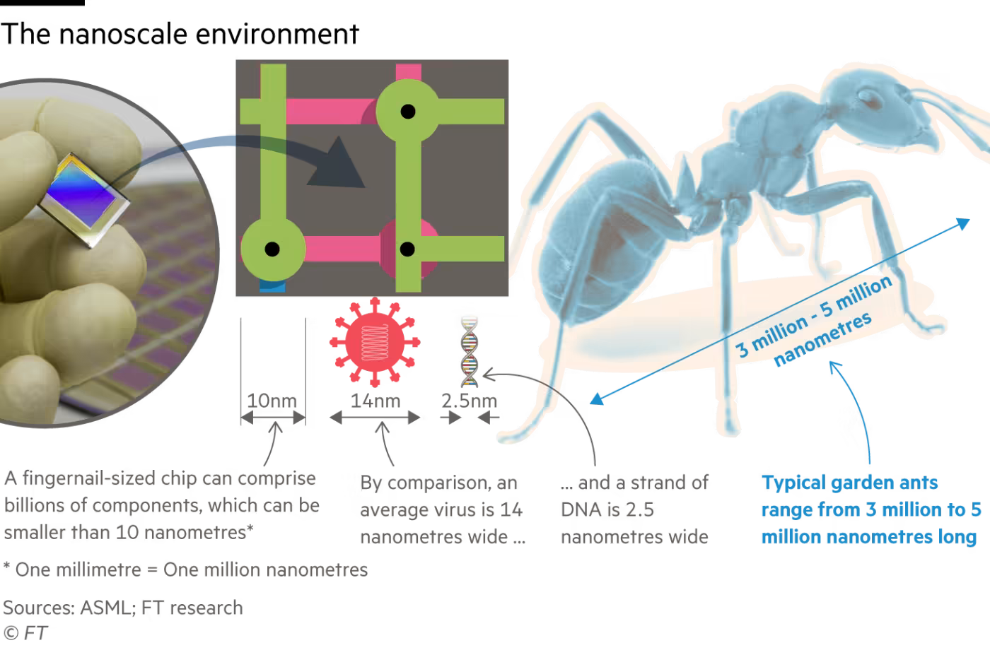
For decades, chipmakers have sought to make ever more compact products. The smaller the transistors on a chip, the lower the energy consumption and the higher their speed. Today, terms such as “2 nanometer” and “3 nanometer” are widely used as shorthand for each new generation of chip, rather than a semiconductor’s actual physical dimensions.
Any company that opens up a technological lead in the next generation of advanced semiconductors will be well placed to dominate an industry that pulled in well over $500 billion in global chip sales last year. That is projected to grow further due to a surge in demand for the data center chips that power generative AI services.
TSMC, which dominates the global market in processors, has already shown the process test results for its “N2”—or 2 nanometer—prototypes to some of its biggest customers, including Apple and Nvidia, according to two people with direct knowledge of the discussions.
But two people close to Samsung said the Korean chipmaker was offering cut-price versions of its latest 2 nanometer prototypes in an effort to attract the interest of big-name customers including Nvidia.
“Samsung sees 2 nanometer as a game-changer,” said James Lim, analyst at US hedge fund Dalton Investments. “But people are still doubtful it can execute the migration better than TSMC.”
Former market leader Intel has also made bold claims about producing its next generation of chips by the end of next year. That could put it back ahead of its Asian rivals, though doubts remain about the performance of the US company’s products.
TSMC, which has said that mass production of N2 chips will begin in 2025, typically launches the mobile version first, with Apple as its lead customer. Versions for PC and then high-performance computing chips designed for higher power loads will come later.
Apple’s latest flagship smartphones, the iPhone 15 Pro and Pro Max, were the first mass-market consumer devices to deploy TSMC’s new 3 nanometer chip technology when they were introduced in September this year.
The challenges of moving from one generation, or “node,” of process technology to the next intensify as chips keep getting smaller, raising the possibility of a misstep that could see TSMC’s crown slip.
TSMC told the Financial Times its N2 technology development was “progressing well and on track for volume production in 2025, and will be the most advanced semiconductor technology in the industry in both density and energy efficiency when it is introduced.”
But Lucy Chen, vice-president of Isaiah Research, noted the cost of moving to the next node was going up, while improvements in performance had plateaued. “Moving to the next generation] is not as attractive to customers anymore,” said Chen.
Experts stress that mass production is still two years away and that teething problems are a natural part of the chip production process.
Insiders at Samsung, which, according to consultancy TrendForce has a 25 percent share of the global advanced foundry market compared with TSMC’s 66 percent, see an opportunity to close the gap.
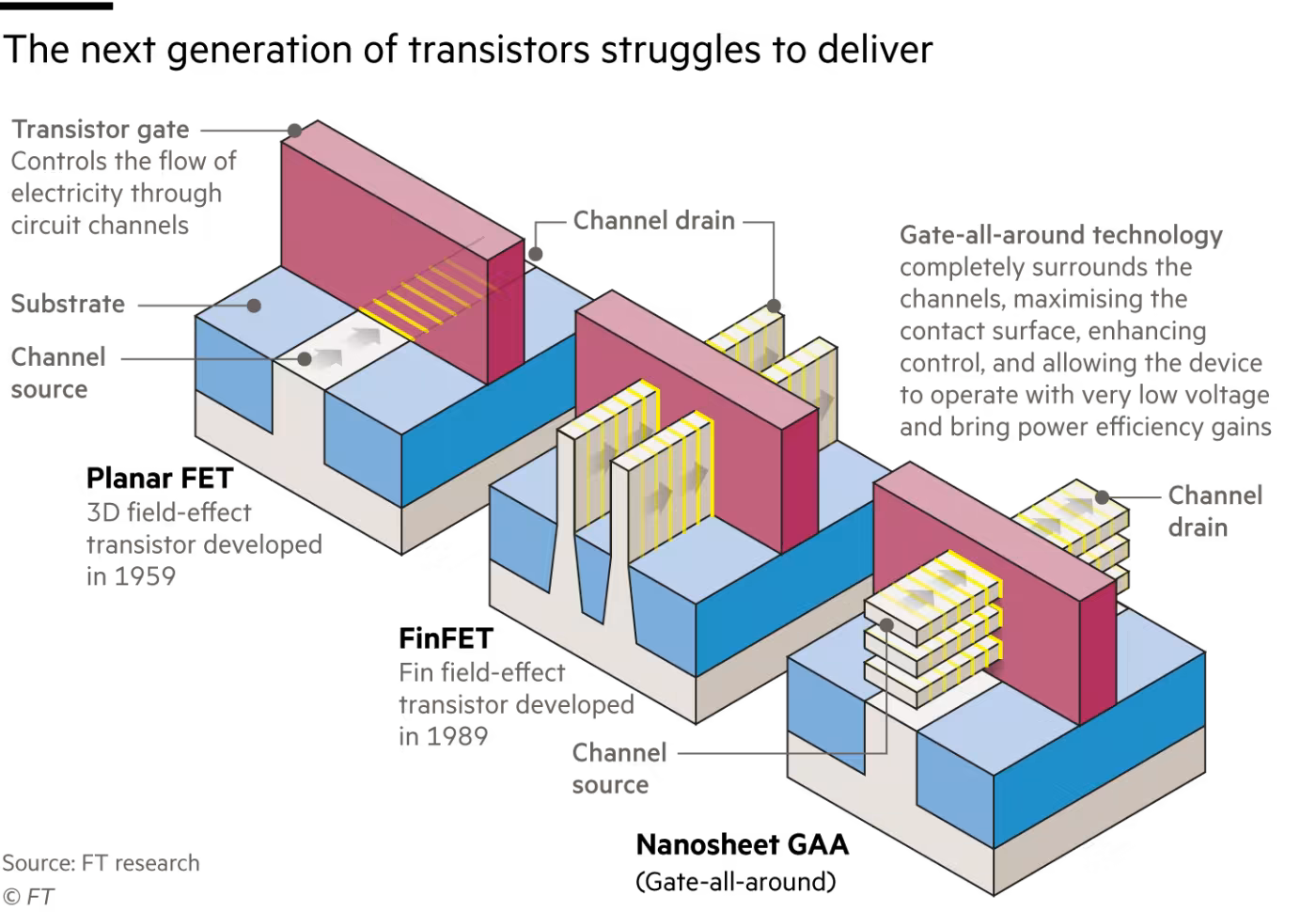
The Korean conglomerate was the first to start mass production of its 3 nm, or “SF3” chips last year, and the first to make the switch to a new transistor architecture known as “Gate-All-Around” (GAA).
According to two people familiar with the situation, US chip designer Qualcomm is planning to use Samsung’s “SF2” chip in its next-generation high-end smartphone processors. That would mark a reversal in fortune after Qualcomm transferred most of its flagship mobile chips from Samsung’s 4 nanometer process to TSMC’s equivalent.
“We are well-equipped to set up for SF2 mass production by 2025,” Samsung said. “Since we were the first to take the leap and transition to GAA architecture, we are hoping the progress from SF3 to SF2 will be relatively seamless.”
Analysts caution that while Samsung was the first to bring its 3 nm chips to market, it has struggled with its “yield rate”—the proportion of chips produced that are deemed shippable to customers.
The Korean company insists that its 3 nanometer yield rates have improved. But according to two people close to Samsung, the yield rate of its simplest 3 nm chip is just 60 percent, well below customer expectations and likely to fall further when producing more complex chips equivalent to Apple’s A17 Pro or Nvidia’s graphic processing units.
“Samsung tries to do these quantum leaps,” said Dylan Patel, chief analyst at research firm SemiAnalysis. “They can claim all they want, but they still have not released a proper 3 nanometer chip.”
Lee Jong-hwan, professor of system semiconductor engineering at Sangmyung University in Seoul, added that Samsung also suffered from the fact that its smartphone and chip design divisions were fierce competitors of the potential customers for the logic chips produced in its foundry division.
“Samsung’s structure causes concern to many potential customers about possible tech or design leaks,” said Lee.
Meanwhile, former market leader Intel is promoting its next generation “18A” node at technology conferences and offering free test production to chip design firms. The US company says it is set to begin production of 18A in late 2024, potentially making it the first chipmaker to migrate to the next generation.
But CC Wei, TSMC’s chief executive, appears unfazed. He said in October that according to the Taiwanese company’s internal assessment its latest 3 nanometer variant, which is already on the market, is comparable to Intel’s 18A in terms of power, performance, and density.
Both Samsung and Intel also hope to benefit from potential customers looking to reduce their dependence on TSMC, whether for commercial reasons or out of concern about a potential Chinese threat to Taiwan. In July, the chief executive of US chipmaker AMD said it would “consider other manufacturing capabilities” besides those offered by TSMC, as it pursued greater “flexibility.”
Leslie Wu, chief executive of consulting firm RHCC, said major customers who require technology at the 2 nanometer level are looking to spread their chip production across multiple foundries. “It’s too risky to rely on TSMC solely.”
But Mark Li, Asia semiconductor analyst at Bernstein, questioned “how meaningful that [geopolitical] factor is compared to factors such as efficiency and schedule is open to debate. TSMC remains superior when it comes to cost, efficiency, and trust.”
The race between Intel, Samsung, and TSMC to ship the first 2 nm chip
Samsung and Intel believe this is their best chance to close the game with TSMC.
Last edited: