Array
(
    [content] => 
    [params] => Array
        (
            [0] => /forum/threads/taiwan-semiconductor-can-lead-until-2032-experts-international-cooperation-strengthens-r-d-security.20543/
        )

    [addOns] => Array
        (
            [DL6/MLTP] => 13
            [Hampel/TimeZoneDebug] => 1000070
            [SV/ChangePostDate] => 2010200
            [SemiWiki/Newsletter] => 1000010
            [SemiWiki/WPMenu] => 1000010
            [SemiWiki/XPressExtend] => 1000010
            [ThemeHouse/XLink] => 1000970
            [ThemeHouse/XPress] => 1010570
            [XF] => 2021770
            [XFI] => 1050270
        )

    [wordpress] => /var/www/html
)

Taiwan Semiconductor can lead until 2032, experts: International cooperation strengthens R&D security

Daniel Nenni

Admin
Staff member
title_bar.gif

Taiwan Semiconductor can lead until 2032, experts: International cooperation strengthens R&D security

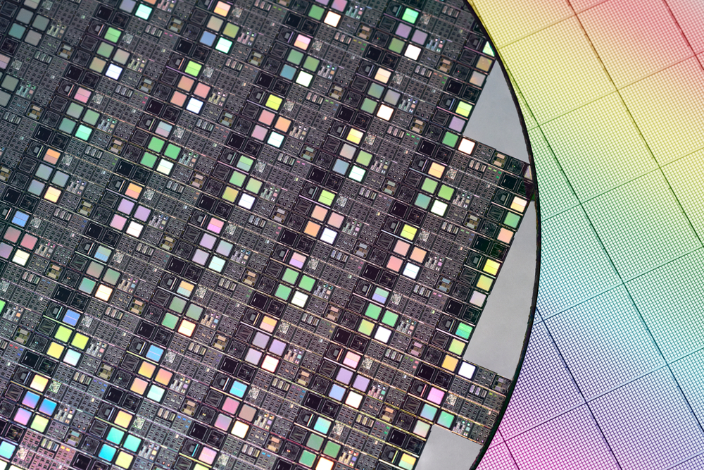
The importance of semiconductors has been elevated to a national security level, and countries around the world, including Europe and the United States, are scrambling to subsidize the development of the semiconductor industry. Yang Ruilin, research director of the International Institute of Obstetrics and Mechanics of the Industrial Research Institute, believes that Taiwan's semiconductor industry is expected to lead until 2032. In terms of next-generation semiconductor technology, Taiwan must cooperate with international companies and strengthen research and development security.

Yang Ruilin said that as geopolitical factors continue to spread, how long Taiwan's semiconductor industry can maintain its competitiveness has attracted much attention from all walks of life. TSMC will mass-produce the 2-nanometer process next year. It is estimated that before the 9-nanometer process technology, both TSMC and Taiwan Semiconductor will maintain their leading position until about 2032.

The next generation of semiconductor technology will have a new chip architecture, and will be deployed in Europe and the United States. Yang Ruilin said that China will also strive to make breakthroughs and achieve independence; Taiwan should cooperate with international cooperation in the future, and in the process, strengthen research and development security and incorporate relevant security mechanisms into the ecosystem.

The "Center for Science, Democracy and Society (DSET)" of the National Science Council today held the annual forum "Taiwan under the Geopolitics of Science and Technology" and invited Yang Ruilin, Global Marketing Director and Taiwan Director of the International Semiconductor Industry Association (SEMI) Cao Shilun, and National Taiwan University Keynote Speakers Yang Guanglei, a visiting professor at the School of Science and Technology, and Xu Zunci, director of the Taiwan Association of Southeast Asian Nations Research Center at the China Economic Research Institute, jointly discussed Taiwan's semiconductor industry and economic security under the geopolitics of technology.

Yang Guanglei reviewed the development of the global semiconductor industry. The United States is the founder of semiconductors, and Moore's Law helped the early development of the U.S. semiconductor industry, making Intel the global semiconductor hegemon and maintaining it for a long time, because the world gathered resources to develop in accordance with Moore's Law.

However, "Success is Moore's Law, and failure is Moore's Law." Yang Guanglei said that Moore's Law promotes industrial division of labor and disintegrates the integrated component manufacturing (IDM) model. Semiconductor manufacturing is developing towards the East because manufacturing conflicts with the American innovation culture. This is the inevitable of the times. The phenomenon.

The United States was overtaken by Japan in the 1980s. Yang Guanglei said that Japan accounted for 50% of the global semiconductor market at its peak. However, the United States could not bear to be replaced, causing Japan to enter a lost 30 years. Not only did it lose its industry, it also caused a talent gap.

Yang Guanglei said that TSMC chose the unfavorable wafer foundry field. Because there was no competition, it was able to grow from a small company to a behemoth company. In the 1990s, Taiwan's stock dividend system attracted a wave of overseas returnees, and the Industrial Research Institute cultivated local talents in Taiwan, promoting the rapid development of the semiconductor industry. The epidemic has disrupted the global supply chain and made the world see the importance of Taiwan's semiconductors.

He pointed out that Taiwan's semiconductor industry is mainly based on manufacturing, and memory is mainly in Japan and South Korea. The upstream part is still dominated by Europe and the United States. Since most upstream companies have developed for nearly 40 years, China has been boycotted by the United States and needs to break through. The difficulty is extremely high, and it is estimated that it may face decades of difficulties.

Geopolitics has both negative obstacles and positive help for Taiwan's semiconductor industry. Yang Guanglei said that the risk mainly comes from the United States, because if the United States wants to reduce the risk of semiconductor manufacturing being concentrated in Asia, it will inevitably require TSMC to manufacture in the United States. Recently, it has been reported that the United States is urging TSMC to go to the United States. R&D, this is not a good thing for Taiwan.

Yang Guanglei said that globalization is dead and Taiwan must face it, maintain Taiwan's competitiveness, continue to develop, and break through unnecessary restrictions. Manufacturing in the United States will cause cost risks, and we should find ways to make up for the cost damage; forward-looking research is the strength of the United States, and we can cooperate with the United States in this regard. We should avoid conflicts with the United States and create lose-lose situations, and we must have intelligent dialogue.

Yang Guanglei said that non-U.S. regions such as Europe and Japan are full of opportunities; as for the huge problem in China, Taiwan may become farther and farther away from China, but China's huge market cannot be ignored. Taiwan should form alliances with countries around the world without compromising its competitiveness.

Yang Guanglei said that Taiwan is not a blue sky without dark clouds. Facing the crisis of declining birthrate, Taiwan should strengthen its productivity; in addition, it should seek a balance between energy and environment.

Regarding the subsidy policy, Yang Guanglei said that subsidies are the worst investment because the one-time subsidy is not enough and the return on investment is very poor. The best investment is investment in forward-looking research. He believes that Taiwan should not subsidize semiconductors as the icing on the cake.

Cao Shilun said that the whole world wants to develop semiconductors, but some countries are in competition with Taiwan. Therefore, Taiwan's semiconductor factories need a grand strategy for their international layout and cooperation, and they should consider taking active or passive strategies.

Xu Zunci emphasized that Taiwan has a complete semiconductor ecosystem and should remain in Taiwan. Facing geopolitical challenges, Taiwan needs a national-level strategy and cross-industry collaboration to find solutions.

 
"It is estimated that before the 9-nanometer process technology, both TSMC and Taiwan Semiconductor will maintain their leading position until about 2032." Seems like a misquote if he did not misspeak.

Probably should be "It is estimated that before the 9-A process technology, both TSMC and Taiwan Semiconductor industry will maintain their leading position until about 2032."
 
8 years is a long time!

If we all take the clock back to 2016 and erase all the obvious things we now know.

TSMC was on 10nm not a great node for them.

Intel was on 14nm.

Who’d have believed that in the next four years TSMC would roar ahead with 7 and 5nm, and set the stage for 3nm and 2nm!

Who’d have believed Intel would go thru 3 CEOs and the senior management churn. Or was it all obvious to those with inside view on both?

Who can really know what is going to happen in 8years, but makes for great gossip
 
8 years is a long time!
If we all take the clock back to 2016 and erase all the obvious things we now know.
TSMC was on 10nm not a great node for them.
Intel was on 14nm.
Who’d have believed that in the next four years TSMC would roar ahead with 7 and 5nm, and set the stage for 3nm and 2nm!
Who’d have believed Intel would go thru 3 CEOs and the senior management churn. Or was it all obvious to those with inside view on both?
Who can really know what is going to happen in 8years, but makes for great gossip

You can thank Apple for that. They push hard and write some very big checks!
 
8 years is a long time!

If we all take the clock back to 2016 and erase all the obvious things we now know.

TSMC was on 10nm not a great node for them.

Intel was on 14nm.

Who’d have believed that in the next four years TSMC would roar ahead with 7 and 5nm, and set the stage for 3nm and 2nm!

Who’d have believed Intel would go thru 3 CEOs and the senior management churn. Or was it all obvious to those with inside view on both?

Who can really know what is going to happen in 8years, but makes for great gossip
In 2014, intel was leading company and launched 2nd generation of FinFET. If we looked at the yield and parameter matching trend, actually it did not ramp smoothly in 14nm. This gave a hint that the launch of 2nd generation of FinFET will not be that smooth. 10nm node was tsmc's 2nd generation FinFET. What tsmc did then was doubling manpower for the development with a project call "Night Eagle". Then it became a big success in 7nm node. We might see the difference in 2014. FYI.
1719877235011.png
 
You can thank Apple for that. They push hard and write some very big checks!
Indeed Apple is one of the important factor of TSMC's success but it's not the only one and not even the most important one. At various time of TSMC's endeavor, there were many decisions, environments, conditions, strategies, engineers, leaders, partners, customers, and visionary ideas that lead to today's TSMC.

Don't forget Apple switched from Samsung to TSMC not because TSMC is cheaper. When AMD, Qualcomm, Nvidia, Google, Amazon, Microsoft, and Facebook chose TSMC instead of Samsung, that's not because TSMC is cheaper either. They all could have written a big prepayment check to Samsung but chose not to do so.

IMO, TSMC's business model, integrity, and people must be listed on the very top of the reasons. Without a clear understanding of this, many governments and companies kept throwing money into semiconductor businesses in hoping to replicate TSMC's success. Most of them failed because they mistakenly thought money, subsidies, even high tariff are the key.
 
Agree there are many factors lead to today tsmc's success not just Apple.
I think Apple's major influences on tsmc are (1) big check (2) the need of incremental but steady improvement every year (3) mindset of absolute deadline to meet iPhone's launch in late Sep every year (4) very robust process to ramp for hundreds of millions iPhone
Intel sadly was given the opportunity, they had scale with >>200 million units, they had profit margin beyond belief, they had products on annual cadence.

Sadly they had a leadership lacking in integrity and customer service and I’d argue still are lacking in customer service and integrity among the leadership
The leadership has improved tbh from BK -> Swan -> Gelsinger the customer service is kind of Mid and some stupid decision still being made
 
Intel sadly was given the opportunity, they had scale with >>200 million units, they had profit margin beyond belief, they had products on annual cadence.

Sadly they had a leadership lacking in integrity and customer service and I’d argue still are lacking in customer service and integrity among the leadership
If Intel took Apple's request for manufacturing chips for iPhone at that time, there's still very high chance Apple and Intel will split up.
The performance/power requirement of SOC is different to CPU, but Intel's processes were optimized for CPU. Also the wafer needed for Apple's A/M chips are 40~50k/month, it's probably double amount of Intel's initial capacity for a new node, which means Intel need to put Apple's priority ahead of internal products. Even in Intel's IDM 2.0 strategy, the new node is still for serving internal products first.
 
If Intel took Apple's request for manufacturing chips for iPhone at that time, there's still very high chance Apple and Intel will split up.
The performance/power requirement of SOC is different to CPU, but Intel's processes were optimized for CPU.
For what it is worth the odd number process (eg P1269) was tailored for SOCs, and the transistor tech lead was so big it gave intel defacto power leadership vs folks like IBM/AMD/GF, I would assume some degree of that would transfer to mobile on an actually competently designed chip. The bigger question is if intel's optimization points would have change if they had an actual incentive to optimize for power rather than Fmax at some TDP in client and perf/watt in server. Maybe; we will never know though. Regardless of that intel did have better cost per FET (a huge deal for mobile APs).
Also the wafer needed for Apple's A/M chips are 40~50k/month
I doubt it is that high. TSMC N5 peak ramp at F18 was sub 100k (memory serves from the numbers Scotten had in 21 it was like 80k), even if we ignore HPC, MTK and QCOM are significantly more than half of the mobile pie. Adding in HPC customers like BCOM, NVIDA, AMD and there is no way Appel could have had that much wafer demand. For older nodes like 16FF there was even less capacity as the market was smaller back then.
it's probably double amount of Intel's initial capacity for a new node, which means Intel need to put Apple's priority ahead of internal products. Even in Intel's IDM 2.0 strategy, the new node is still for serving internal products first.
Apple die sizes on A series are generally well under 100mm2. Intel client parts tend to be around 100-150 (before node scaling stalled due to 10nm and 7nm delays), and DC products are always much much larger (400-600mm2 range). On a unit basis Apple sells let's call it 205M iphones a year on avg during the period in question. Let's say that 1/4 are old gen, that gives us 154M units a year on the newest node. In 2018 there were 55.37M PCs. For rounding sake let's say 95% are intel CPUs (52.6M). Blueone said server was a 30M a year market in they heydays. Let's say 80% of client and 60% of server is on the newest node. That is 60M units. Each of those server dies requires far more wafers than client chips due to lower yield and fewer DPW. Let say avg intel wafer has a die size of 200mm2 that is conservatively 2x avg Apple die. By that measurement intel CPU logic only demand is 78% of Apple assuming no yield rolloff from larger die sizes (bad assumption but I can't be bothered to do that math). I'm not counting iPAD sales (which if memory serves just used A series not M series back then) so we'll call it even. There is also the chipset that get sold with the intel CPUs (mobo chipset, PCH die on laptops, WIFI, bluetooth, TB controller, cellular modems, and more stuff that I have prob never heard of) and those historically started appearing on the new node 1yr after the CPUs (hence having some overlap with leading edge CPUs).

Another way of looking at it is number of fabs. If we ignore D1D since it is a pilot factory you have 4 fabs on 22nm. For F18 TSMC had 3 or 4 fabs churning N5 (I don't think there is exact confirmation on how many there were, but we know at least 3 since that is how many were operational in 2021). Granted D1C and F12 are smaller than a F18 phase, but the technology had a MUCH shorter flow, N5 was the fastest ramp in TSMC history pre N3, and a D1D style fab (F32/28) seem to be similar in size to a tad bigger than a TSMC F18 phase.

Sources:
1719975725683.png

1719974948657.png

1720009704645.png


Last edited:
I doubt it is that high. TSMC N5 peak ramp at F18 was sub 100k (memory serves from the numbers Scotten had in 21 it was like 80k), even if we ignore HPC, MTK and QCOM are significantly more than half of the mobile pie. Adding in HPC customers like BCOM, NVIDA, AMD and there is no way Appel could have had that much wafer demand. For older nodes like 16FF there was even less capacity as the market was smaller back then.
Great thanks for details calculation. My impression was coming from news that tsmc usually have ~50k wafers/month for initial stage of a new node. And news usually stated the 1st year capacity is not enough for Qualcomm/MediaTek.
 
Great thanks for details calculation. My impression was coming from news that tsmc usually have ~50k wafers/month for initial stage of a new node. And news usually stated the 1st year capacity is not enough for Qualcomm/MediaTek.

Just went to check, and N5 peak ramp fat fab18 would have likely been in that 140k range and at least 120k (per fig 1 in this post). Oddly seems counter to TSMC's numbers in fig 2, so I don't exactly know what to think on the ICK numbers given the ratios don't match TSMC's. Either way I did misremember the capacity numbers from this ICK chart. The rest of the numbers would be unchanged though as the number of fabs working on the technology is known, and the estimations of relative wafer demands Apple vs intel would be unchanged (since my methodology was working backwards from sales).

As for initial Apple ramp if we do take 50k WSPM, not all of that will be for Apple. Given how many customers and IP partners work with TSMC, when a node is brand new there is likely non trivial amount of capacity of customer testchips and cert vehicles flying around. When F12 transfers the technology F18 also becomes responsible for process development (yield enhancement, performance enhancement, customization for customers, sub variants like RF, LL, HV, MRAM, etc) which also uses up significant capacity even if we assume that at this point most of the yield learning is done on product rather than on TD testchips dedicated to stressing the process corners. Final thing on that is capacity can be sacrificed for velocity. For TCs and TD wafers they are almost certainly run as hot boxes. For the early launch volume I don't assume Apple HB material thru the line to make sure they have lots of phones at launch since that would be VERY expensive for Apple, but you never know. "Why hold up a $1000 phone on a $40 chip".
1720008969275.png


1720009739799.png
 
For what it is worth the odd number process (eg P1269) was tailored for SOCs, and the transistor tech lead was so big it gave intel defacto power leadership vs folks like IBM/AMD/GF, I would assume some degree of that would transfer to mobile on an actually competently designed chip. The bigger question is if intel's optimization points would have change if they had an actual incentive to optimize for power rather than Fmax at some TDP in client and perf/watt in server. Maybe; we will never know though. Regardless of that intel did have better cost per FET (a huge deal for mobile APs).

I doubt it is that high. TSMC N5 peak ramp at F18 was sub 100k (memory serves from the numbers Scotten had in 21 it was like 80k), even if we ignore HPC, MTK and QCOM are significantly more than half of the mobile pie. Adding in HPC customers like BCOM, NVIDA, AMD and there is no way Appel could have had that much wafer demand. For older nodes like 16FF there was even less capacity as the market was smaller back then.

Apple die sizes on A series are generally well under 100mm2. Intel client parts tend to be around 100-150 (before node scaling stalled due to 10nm and 7nm delays), and DC products are always much much larger (400-600mm2 range). On a unit basis Apple sells let's call it 205M iphones a year on avg during the period in question. Let's say that 1/4 are old gen, that gives us 154M units a year on the newest node. In 2018 there were 55.37M PCs. For rounding sake let's say 95% are intel CPUs (52.6M). Blueone said server was a 30M a year market in they heydays. Let's say 80% of client and 60% of server is on the newest node. That is 60M units. Each of those server dies requires far more wafers than client chips due to lower yield and fewer DPW. Let say avg intel wafer has a die size of 200mm2 that is conservatively 2x avg Apple die. By that measurement intel CPU logic only demand is 78% of Apple assuming no yield rolloff from larger die sizes (bad assumption but I can't be bothered to do that math). I'm not counting iPAD sales (which if memory serves just used A series not M series back then) so we'll call it even. There is also the chipset that get sold with the intel CPUs (mobo chipset, PCH die on laptops, WIFI, bluetooth, TB controller, cellular modems, and more stuff that I have prob never heard of) and those historically started appearing on the new node 1yr after the CPUs (hence having some overlap with leading edge CPUs).

Another way of looking at it is number of fabs. If we ignore D1D since it is a pilot factory you have 4 fabs on 22nm. For F18 TSMC had 3 or 4 fabs churning N5 (I don't think there is exact confirmation on how many there were, but we know at least 3 since that is how many were operational in 2021). Granted D1C and F12 are smaller than a F18 phase, but the technology had a MUCH shorter flow, N5 was the fastest ramp in TSMC history pre N3, and a D1D style fab (F32/28) seem to be similar in size to a tad bigger than a TSMC F18 phase.

Sources:
View attachment 2073
View attachment 2072
View attachment 2075


Another way to look into this Apple related TSMC wafer production is to analyze the wafer quantity needed to support Apple's sales. Here I use 2023 iPhone, Macs, and iPads' worldwide shipment to calculate the possible minimum TSMC wafer output needed.

My die cut per wafer estimate is probably on the higher end of the actual number. To simplify the calculation, I assume 100% yield with no damage or loss through the whole Apple supply chain operations. You can plug in your own number to make it more close to the situation you believed.

My estimate is that averagely Apple bought at least 63,221 units of 12-inch equivalent wafers per month from TSMC in 2023. Majority of them were produced at TSMC Fab18 in Tainan Taiwan using TSMC N3 and N5/N4 technologies. Apple Watch, Apple TV, iPods and many other chips needed in the Apple products are not included in this analysis.


1720027019973.png
 
Last edited:
Just went to check, and N5 peak ramp fat fab18 would have likely been in that 140k range and at least 120k (per fig 1 in this post). Oddly seems counter to TSMC's numbers in fig 2, so I don't exactly know what to think on the ICK numbers given the ratios don't match TSMC's. Either way I did misremember the capacity numbers from this ICK chart. The rest of the numbers would be unchanged though as the number of fabs working on the technology is known, and the estimations of relative wafer demands Apple vs intel would be unchanged (since my methodology was working backwards from sales).

As for initial Apple ramp if we do take 50k WSPM, not all of that will be for Apple. Given how many customers and IP partners work with TSMC, when a node is brand new there is likely non trivial amount of capacity of customer testchips and cert vehicles flying around. When F12 transfers the technology F18 also becomes responsible for process development (yield enhancement, performance enhancement, customization for customers, sub variants like RF, LL, HV, MRAM, etc) which also uses up significant capacity even if we assume that at this point most of the yield learning is done on product rather than on TD testchips dedicated to stressing the process corners. Final thing on that is capacity can be sacrificed for velocity. For TCs and TD wafers they are almost certainly run as hot boxes. For the early launch volume I don't assume Apple HB material thru the line to make sure they have lots of phones at launch since that would be VERY expensive for Apple, but you never know. "Why hold up a $1000 phone on a $40 chip".
View attachment 2074

View attachment 2076

According to TSMC website and 2023 Annual report:

1. Total wafer shipments (2023) were 12.0 million 12-inch equivalent wafers as compared to 15.3 million 12-inch equivalent wafers in 2022.
  • 2. Advanced technologies (7-nanometer and beyond) accounted for 58 percent of total wafer revenue, up from 53 percent in 2022.
3. Annual capacity of the manufacturing facilities managed by TSMC and its subsidiaries exceeded 16 million 12-inch equivalent wafers in 2023. These facilities include four 12-inch wafer GIGAFAB® fabs, four 8-inch wafer fabs, and one 6-inch wafer fab – all in Taiwan – as well as one 12-inch wafer fab at a wholly owned subsidiary, TSMC Nanjing Company Limited, and two 8-inch wafer fabs at wholly owned subsidiaries, TSMC Washington in the United States and TSMC China Company Limited.

4. The Company currently operates four 12-inch GIGAFAB® facilities – Fab 12, 14, 15 and 18. The combined capacity of the four facilities exceeded 12 million 12-inch wafers in 2023. Production within these facilities support 0.13μm, 90nm, 65nm, 40nm, 28nm, 16nm, 7nm, 5nm and 3nm process technologies and their sub-nodes.

My comments:

TSMC F18 (N3, N5) and Fab15 (N7 and N20) are two most important fabs for leading edge node production. I think the 2023 wafer output between Fab18 and Fab15 could exceed 4.3 million 12-inch wafers. Fab18 alone probably produced around 2.6 million 12-inch wafers in 2023 across N3 and N5, or 217,000 12-inch wafers monthly in 2023 across N3 and N5
 
Another way to look into this Apple related TSMC wafer production is to analyze the wafer quantity needed to support Apple's sales. Here I use 2023 iPhone, Macs, and iPads' worldwide shipment to calculate the possible minimum TSMC wafer output needed.
I was using old data because we were talking about the period where intel fell behind. The scale disparity is much different in this day and age (somethings help Apple here and others hurt). For example Apple uses the new SOC only in the pro phones and then it rolls out to the mainstream the year after (this heavily blunts wafer demand in year 0). Apple now does their own PC CPUs. The mobile market and PC markets are slightly bigger than back then. Intel die sizes on client products have over doubled and Xeons are like triple the size. Disag hurts intel leading edge wafer demands, intel chipsets are often made externally now, CPUs and GPUs are external as well.
My die cut per wafer estimate is probably on the higher end of the actual number. To simplify the calculation, I assume 100% yield with no damage or loss through the whole Apple supply chain operations. You can plug in your own number to make it more close to the situation you believed.

My estimate is that averagely Apple bought at least 63,221 units of 12-inch equivalent wafers per month from TSMC in 2023. Majority of them were produced at TSMC Fab18 in Tainan Taiwan using TSMC N3 and N5/N4 technologies. Apple Watch, Apple TV, iPods and many other chips needed in the Apple products are not included in this analysis.


View attachment 2078
DPW for A series are too low especially on N5 where yields are very mature. As an example the recent A14 (first N5 chip) is 88mm2 and you can fit just shy of 700 per wafer. Mac and iPAD number feels like it would be too high, did you have a source for the Mac and ipad shipments? My understanding is that most or maybe all ipads use M-series these days not A series SOCs. Mac dpw are also a way too low, the lions share of the volume is ultra portable Mx rather than the Pro or Ultra. The M4 which is used for ipads and the vast majority of mac volume is 169mm2 and you can fit around 330 of them per wafer, and for reference M1 was about 118mm2 (489 dpw).
 
I was using old data because we were talking about the period where intel fell behind. The scale disparity is much different in this day and age (somethings help Apple here and others hurt). For example Apple uses the new SOC only in the pro phones and then it rolls out to the mainstream the year after (this heavily blunts wafer demand in year 0). Apple now does their own PC CPUs. The mobile market and PC markets are slightly bigger than back then. Intel die sizes on client products have over doubled and Xeons are like triple the size. Disag hurts intel leading edge wafer demands, intel chipsets are often made externally now, CPUs and GPUs are external as well.

DPW for A series are too low especially on N5 where yields are very mature. As an example the recent A14 (first N5 chip) is 88mm2 and you can fit just shy of 700 per wafer. Mac and iPAD number feels like it would be too high, did you have a source for the Mac and ipad shipments? My understanding is that most or maybe all ipads use M-series these days not A series SOCs. Mac dpw are also a way too low, the lions share of the volume is ultra portable Mx rather than the Pro or Ultra. The M4 which is used for ipads and the vast majority of mac volume is 169mm2 and you can fit around 330 of them per wafer, and for reference M1 was about 118mm2 (489 dpw).

"As an example the recent A14 (first N5 chip) is 88mm2 and you can fit just shy of 700 per wafer."

One of the reasons I didn't use that A14 number is that A14 was released in 2020. By the end of 2023 (the data year I did my estimate), A15 (108.01 mm2, N5P, 2021), A16 (112.75 mm2, N4P, 2022), and A17 Pro (103.80 mm2. N3B, 2023) were all released and probably formed the majority of TSMC 2023 Apple A series production. Hope one day Apple can donate a production wafer for each edition of the Apple Silicon to a science museum then the truth can be told.

Feel free to use whatever number you think is more close to the real situation and share your estimate with us. :)
 
Back
Top