Semiconductor manufacturer STMicroelectronics will see up to 2,800 employees leave the company globally over the next three years as part of an overhaul of its manufacturing operations and cost structure.
The company announced the voluntary workforce reduction in a press release as it detailed a major restructuring initiative aimed at modernising facilities, boosting automation, and increasing efficiency across its manufacturing network.The job cuts, which will occur in addition to normal staff turnover, are expected to mainly take place in 2026 and 2027. ST says that these will be managed exclusively through voluntary measures, and through dialogue and negotiations with employee representatives – in compliance with national regulations.
“The reshaping of our manufacturing footprint announced today will future proof our Integrated Device Manufacturer model with strategic assets in Europe and improve our ability to innovate even faster, benefitting all our stakeholders. As we focus on advanced manufacturing infrastructure and mainstream technologies, we will continue to leverage all of our existing sites and bring redefined missions for some of them to support their long-term success,” says ST CEO Jean-Marc Chery, in the press release.
STMicroelectronics' manufacturing overhaul has two main goals: to prioritise investment in advanced infrastructure like 300mm silicon and 200mm silicon carbide fabs, and to improve efficiency in existing 150mm and mature 200mm facilities. At the same time, the company will continue upgrading its operations with new technologies, including AI and automation. ST expects the changes to unlock high triple-digit million-dollar cost savings annually by the end of 2027.
Reshaping its manufacturing footprint
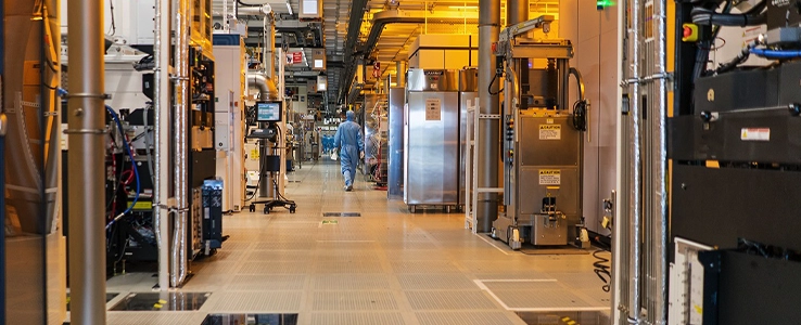
STMicroelectronics’ restructuring will affect nearly all of its global manufacturing sites, with a focus on scaling advanced capabilities and reallocating resources for greater efficiency.
In Agrate, Italy, the 300mm wafer fabrication plant will continue to be scaled up, aiming to become the company’s flagship high-volume site for smart power and mixed-signal technologies. Capacity is set to double to 4,000 wafers per week by 2027, with planned modular expansions increasing capacity up to 14,000 wpw, depending on market conditions. The adjacent 200mm facility will shift its focus to MEMS production.
In Crolles, France, the 300mm fab is also set for expansion, targeting a capacity of 14,000 wafers per week by 2027, with the potential to scale up to 20,000 wafers per week. ST plans to repurpose the existing 200mm fab to support Electrical Wafer Sorting high volume manufacturing and advanced packaging technologies, hosting activities not currently present in Europe. Focus will be on next-gen leading technologies including optical sensing and silicon photonics.
In Catania, Italy, ST will maintain its focus on power and wide-bandgap semiconductors. The development of the new Silicon Carbide Campus is said to be on track, with 200mm wafer production expected to begin in the fourth quarter of 2025. The site will shift resources from 150mm and Electrical Wafer Sorting activities towards 200mm silicon carbide and silicon power semiconductor production, including GaN-on-silicon.
Other facilities will also undergo optimisation
Rousset, France will remain focused on 200mm production, with additional volumes reallocated from other locations to fully utilise existing capacity.
Tours, France will remain focused on its 200mm silicon production line for select technologies. Legacy 150mm activities will be relocated, while the site retains its role as a centre of competence for GaN epitaxy. Tours will also take on a new strategic function in panel-level packaging.
Ang Mo Kio, Singapore will remain ST’s core site for high-volume mature technologies, will remain focused on 200mm silicon manufacturing and will also host our consolidated global legacy 150mm silicon capabilities.
Kirkop, Malta, ST’s European test and packaging site, will be upgraded with advanced automation to support the production of next-generation semiconductor products.
ST to cut up to 2,800 jobs in major manufacturing overhaul
Semiconductor manufacturer STMicroelectronics will see up to 2,800 employees leave the company globally over the next three years as part of an overhaul of its manufacturing operations and cost structure.
 evertiq.com
