- Establishing a dedicated development organization in the semiconductor research institute
- Mass production is expected to begin after 2029
- TSMC Announces 1.6nm Production Next Year

Photo = Created by OpenAI 'Dali'
Samsung Electronics has started developing the 1.0㎚ (nanometer, 1 billionth of a meter) foundry process, which is called the dream semiconductor process. As there is a realistic gap with Taiwan's TSMC in technologies that are close to mass production, such as the 2㎚ process, the company plans to speed up the development of the 1㎚ process, a future technology, to create an opportunity for a turnaround.
According to industry sources on the 9th, Samsung Electronics Semiconductor Research Institute recently began developing a 1.0 nanometer process. Some researchers who participated in the development of cutting-edge processes such as 2 nanometers were transferred to form a project team. 1.0 nanometers is called the dream semiconductor process, and in the foundry process roadmap that Samsung Electronics has released so far, the 1.4 nanometer process scheduled for mass production in 2027 is the most advanced.
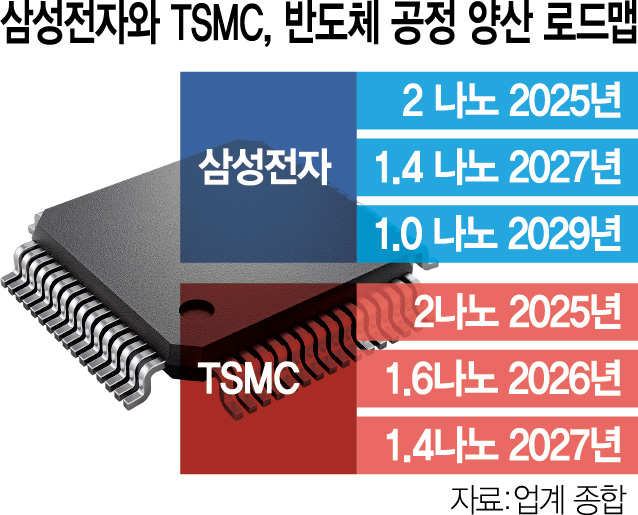
The 1.0 nanometer process requires a new technology concept that breaks the mold of existing designs as well as the introduction of next-generation equipment such as high-NA EUV exposure equipment. The company is targeting mass production after 2029.
Samsung Electronics is lagging behind TSMC in its technological prowess in the 3 nanometer process that is currently in mass production and the 2 nanometer process that is scheduled for mass production this year, so expectations for the 1 nanometer process are high. In the case of 2 nanometers, TSMC’s yield has already exceeded 60%, and the gap with Samsung Electronics is not small. In particular, it was reported that Chairman Lee Jae-yong started development of the 1 nanometer process early last month after urging executives to “continue the tradition of prioritizing technology” and emphasizing, “Let’s create the future with technology that doesn’t exist in the world.”
Competitors are also accelerating the development of 1 nanometer processes. Last April, TSMC made a surprise announcement that it would add 16A technology, meaning 1.6 nanometers, between the existing 1.4 nanometers and 2 nanometers and start production in the second half of 2026. This is an analysis that it is responding to the technological demand of the rapidly changing artificial intelligence (AI) semiconductor market and laying the foundation for the next-generation process.
Samsung Foundry Division, which recently replaced its leadership, is focusing on expanding its business ecosystem while strengthening its technological capabilities. Jin-man Han, head and president of Samsung Electronics Foundry Division, has recently been focusing on strengthening partnerships by meeting with domestic AI semiconductor startups such as DeepX to understand customer needs.
 www.sedaily.com
- Mass production is expected to begin after 2029
- TSMC Announces 1.6nm Production Next Year
Photo = Created by OpenAI 'Dali'
Samsung Electronics has started developing the 1.0㎚ (nanometer, 1 billionth of a meter) foundry process, which is called the dream semiconductor process. As there is a realistic gap with Taiwan's TSMC in technologies that are close to mass production, such as the 2㎚ process, the company plans to speed up the development of the 1㎚ process, a future technology, to create an opportunity for a turnaround.
According to industry sources on the 9th, Samsung Electronics Semiconductor Research Institute recently began developing a 1.0 nanometer process. Some researchers who participated in the development of cutting-edge processes such as 2 nanometers were transferred to form a project team. 1.0 nanometers is called the dream semiconductor process, and in the foundry process roadmap that Samsung Electronics has released so far, the 1.4 nanometer process scheduled for mass production in 2027 is the most advanced.
The 1.0 nanometer process requires a new technology concept that breaks the mold of existing designs as well as the introduction of next-generation equipment such as high-NA EUV exposure equipment. The company is targeting mass production after 2029.
Samsung Electronics is lagging behind TSMC in its technological prowess in the 3 nanometer process that is currently in mass production and the 2 nanometer process that is scheduled for mass production this year, so expectations for the 1 nanometer process are high. In the case of 2 nanometers, TSMC’s yield has already exceeded 60%, and the gap with Samsung Electronics is not small. In particular, it was reported that Chairman Lee Jae-yong started development of the 1 nanometer process early last month after urging executives to “continue the tradition of prioritizing technology” and emphasizing, “Let’s create the future with technology that doesn’t exist in the world.”
Competitors are also accelerating the development of 1 nanometer processes. Last April, TSMC made a surprise announcement that it would add 16A technology, meaning 1.6 nanometers, between the existing 1.4 nanometers and 2 nanometers and start production in the second half of 2026. This is an analysis that it is responding to the technological demand of the rapidly changing artificial intelligence (AI) semiconductor market and laying the foundation for the next-generation process.
Samsung Foundry Division, which recently replaced its leadership, is focusing on expanding its business ecosystem while strengthening its technological capabilities. Jin-man Han, head and president of Samsung Electronics Foundry Division, has recently been focusing on strengthening partnerships by meeting with domestic AI semiconductor startups such as DeepX to understand customer needs.
[단독] 삼성전자, ‘꿈의 반도체 공정’ 1나노 첫 개발 돌입
산업 > 산업일반 뉴스: 삼성전자(005930)가 꿈의 반도체 공정으로 불리는 1.0㎚(나노미터·10억분의 1m) 파운드리 공정 개발에 착수했다. 2나노 ...
www.sedaily.com

")