Samsung Electronics, Electrical Engineering, and Display begin joint R&D
Reduced thickness and heat-resistant packaging material in all-out effort to ‘commercialize’ faster than Intel

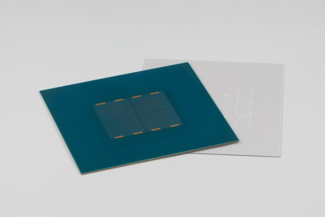
Samsung Electro-Mechanics glass substrate. Photo provided by Samsung Electro-Mechanics
Samsung Group's electronic affiliates formed a united front and began joint research and development (R&D) to accelerate the commercialization of 'glass substrate', which is called the dream substrate. The strategy is to succeed in commercialization faster than Intel, a semiconductor rival company that entered glass substrate R&D 10 years ago. As packaging has emerged as the biggest issue in the semiconductor industry, competition for leadership in packaging materials as well as chip miniaturization is fierce.
According to the industry on the 12th, Samsung Electro-Mechanics has begun joint R&D on glass substrates with the group's major electronic affiliates, including Samsung Electronics and Samsung Display.
Samsung Electronics is expected to take on the know-how for combining semiconductors and substrates, and Samsung Display is expected to take on roles such as glass processing. This is the first time that Samsung Electro-Mechanics is known to be conducting glass substrate research together with electronic component affiliates such as Samsung Electronics and Samsung Display. At CES 2024 in January, Samsung Electro-Mechanics presented a goal of “mass production of glass substrates in 2026.” An industry official said, “As each company possesses the world’s best technology, synergies will be maximized in glass substrate research, which is a promising field,” and added, “It is also important to watch how the glass substrate ecosystem of Samsung’s joint venture will be established.”
A glass substrate is a semiconductor substrate that optimizes the connection between chips and electronic devices. Compared to existing plastic boards, the thickness can be reduced by carving finer circuits, and it is heat resistant, making it advantageous for large-area and high-performance chip combinations.
A strong rival of the glass substrate Samsung alliance is Intel of the United States. In September of last year, Intel announced, “We will mass produce glass substrates by 2030.” They invested $1 billion (approximately 1.3 trillion won) in their Arizona factory 10 years ago to establish a glass substrate R&D line and establish a supply chain. Japan's Ibiden, the world's No. 1 semiconductor substrate manufacturer, also announced in October last year that it was targeting glass substrates as a new business and was engaging in R&D. In Korea, SKC, an affiliate of SK Group, has established a subsidiary, Absolix, and is exploring mass production of substrates with the world's top semiconductor companies, such as AMD.

 sedaily.com
Reduced thickness and heat-resistant packaging material in all-out effort to ‘commercialize’ faster than Intel

Samsung Electro-Mechanics glass substrate. Photo provided by Samsung Electro-Mechanics
Samsung Group's electronic affiliates formed a united front and began joint research and development (R&D) to accelerate the commercialization of 'glass substrate', which is called the dream substrate. The strategy is to succeed in commercialization faster than Intel, a semiconductor rival company that entered glass substrate R&D 10 years ago. As packaging has emerged as the biggest issue in the semiconductor industry, competition for leadership in packaging materials as well as chip miniaturization is fierce.
According to the industry on the 12th, Samsung Electro-Mechanics has begun joint R&D on glass substrates with the group's major electronic affiliates, including Samsung Electronics and Samsung Display.
Samsung Electronics is expected to take on the know-how for combining semiconductors and substrates, and Samsung Display is expected to take on roles such as glass processing. This is the first time that Samsung Electro-Mechanics is known to be conducting glass substrate research together with electronic component affiliates such as Samsung Electronics and Samsung Display. At CES 2024 in January, Samsung Electro-Mechanics presented a goal of “mass production of glass substrates in 2026.” An industry official said, “As each company possesses the world’s best technology, synergies will be maximized in glass substrate research, which is a promising field,” and added, “It is also important to watch how the glass substrate ecosystem of Samsung’s joint venture will be established.”
A glass substrate is a semiconductor substrate that optimizes the connection between chips and electronic devices. Compared to existing plastic boards, the thickness can be reduced by carving finer circuits, and it is heat resistant, making it advantageous for large-area and high-performance chip combinations.
A strong rival of the glass substrate Samsung alliance is Intel of the United States. In September of last year, Intel announced, “We will mass produce glass substrates by 2030.” They invested $1 billion (approximately 1.3 trillion won) in their Arizona factory 10 years ago to establish a glass substrate R&D line and establish a supply chain. Japan's Ibiden, the world's No. 1 semiconductor substrate manufacturer, also announced in October last year that it was targeting glass substrates as a new business and was engaging in R&D. In Korea, SKC, an affiliate of SK Group, has established a subsidiary, Absolix, and is exploring mass production of substrates with the world's top semiconductor companies, such as AMD.

[단독] '유리 기판' 초격차…삼성 연합군 뜬다
삼성그룹의 전자 계열사들이 꿈의 기판으로 일컬어지는 ‘유리 기판’ 상용화를 앞당기기 위해 연합 전선을 구축하고 공동 연구...
 sedaily.com
