Nvidia's next-generation AI chips, the Blackwell series, recently sparked a stir with reports of shipment delays. On November 17, international media further reported that the servers designed for the Blackwell chips are experiencing overheating issues. Nvidia is currently requesting suppliers to redesign these systems to address the problem, but clients are worried about insufficient time to prepare new data centers.

According to The Information, Nvidia's Blackwell GPUs revealed potential overheating risks in servers equipped with 72 cores. These servers are expected to consume up to 120 kW per rack, and the overheating issue not only limits GPU performance but could also damage components. As a result, Nvidia has repeatedly reassessed the design of server racks.

The Challenges with GB200 Chip Design
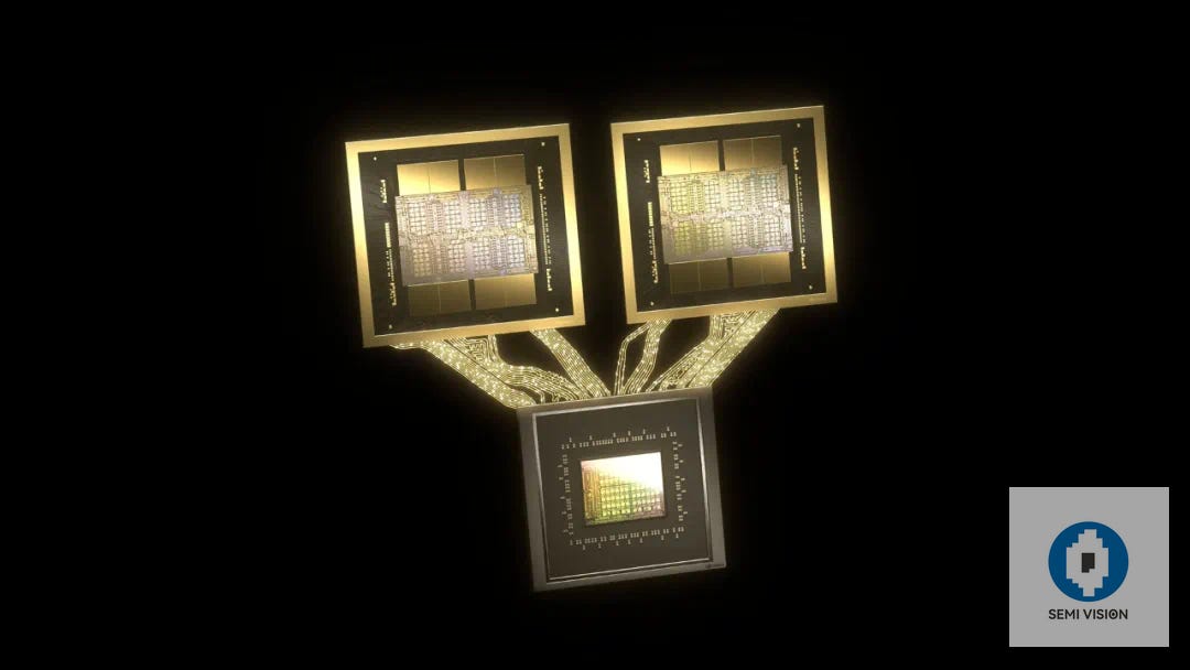
In August, reports surfaced regarding design flaws in the Blackwell series. Notably, Blackwell is Nvidia's first GPU to adopt a Multi-Chip Module (MCM) design, integrating two GPUs on a single chip. This "2-in-1" innovation evidently cannot rely on traditional manufacturing methods. The B100 and B200 GPU models of the Blackwell series employ TSMC's CoWoS-L packaging technology to link the two chips, leveraging a Redistribution Layer (RDL) interposer with localized silicon interconnects (LSI) to achieve data transfer rates of approximately 10 TB/s.

TSMC CoWoS Introduction
However, discrepancies in thermal expansion characteristics among the GPU chips, LSI bridges, RDL interposers, and motherboard substrates lead to structural warping in the packaging, triggering system failures.
Currently, the GB200 chip design poses significant challenges due to its large size and high power consumption. With a single die area of approximately 800–900 mm² and a power range of 400–600 W, GB200 ranks among the largest AI/HPC chips in the industry. Its substantial size stems from the high transistor density per unit area, enabling exceptional performance.
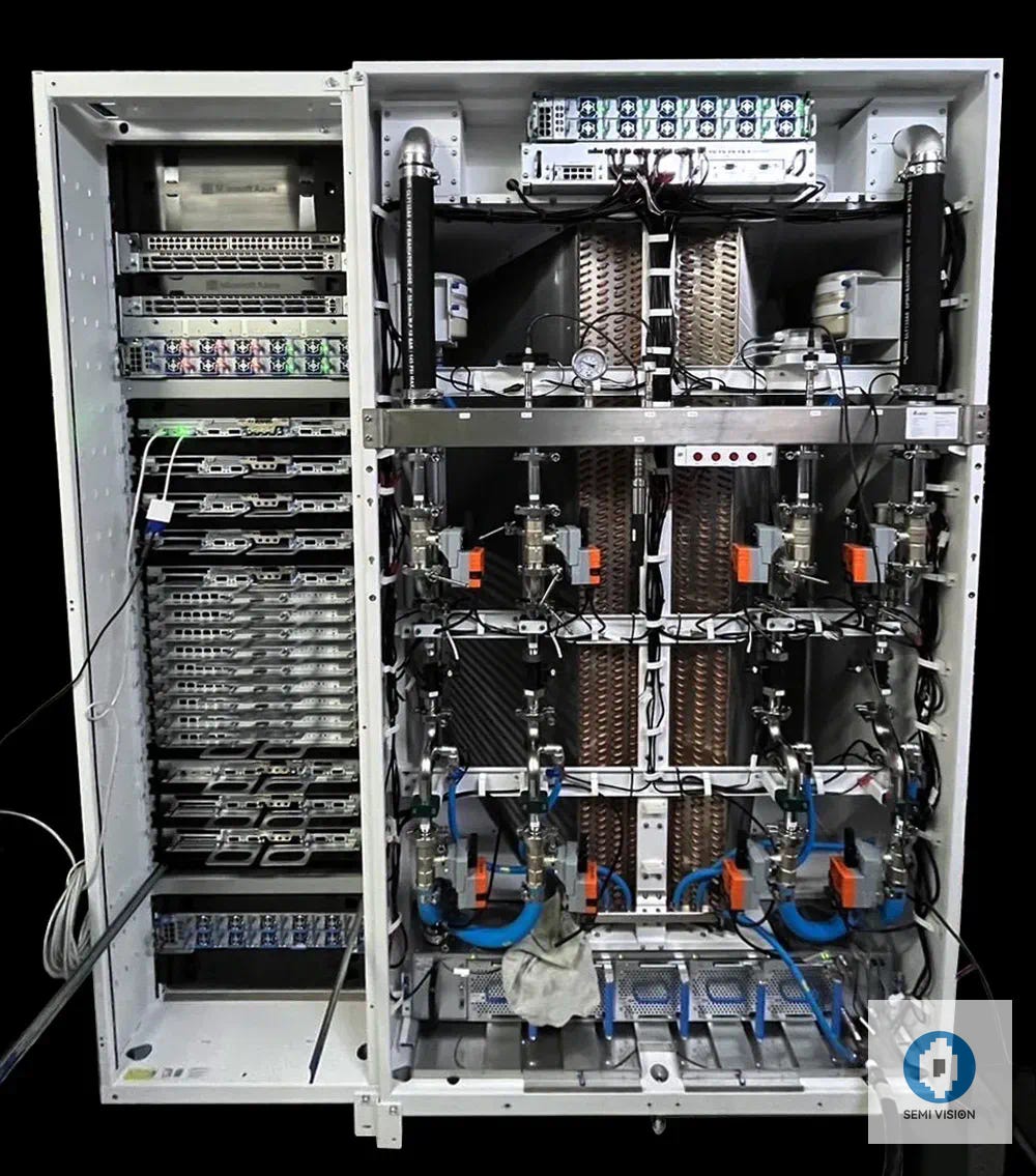
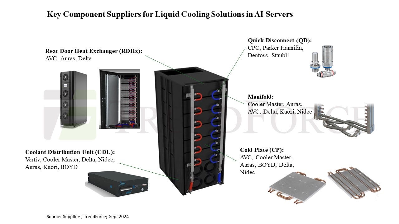
To manage the heat generated by such chips, high-efficiency cooling systems like liquid cooling are necessary. These systems use water cooling plates to transfer heat from the chip through microfluid channels that enable heat exchange between cold and hot water. The key component here is the Cooling Distribution Unit (CDU), which regulates and distributes the coolant flow throughout the system. Working alongside pumps, radiators, heat exchangers, and controllers, the CDU ensures efficient cooling. Additionally, it filters out impurities to prevent clogging or damage to other components.
The CDU directs water through manifolds into the cooling plates. This process is akin to supplying water to every floor of a skyscraper, where sufficient water pressure is required to ensure that cold water reaches even the top levels. However, excessive pressure could lead to leakage, creating a physical limitation.

Why Data Centers Need Liquid Cooling ?

Source: ASE

 tspasemiconductor.substack.com
According to The Information, Nvidia's Blackwell GPUs revealed potential overheating risks in servers equipped with 72 cores. These servers are expected to consume up to 120 kW per rack, and the overheating issue not only limits GPU performance but could also damage components. As a result, Nvidia has repeatedly reassessed the design of server racks.
The Challenges with GB200 Chip Design
In August, reports surfaced regarding design flaws in the Blackwell series. Notably, Blackwell is Nvidia's first GPU to adopt a Multi-Chip Module (MCM) design, integrating two GPUs on a single chip. This "2-in-1" innovation evidently cannot rely on traditional manufacturing methods. The B100 and B200 GPU models of the Blackwell series employ TSMC's CoWoS-L packaging technology to link the two chips, leveraging a Redistribution Layer (RDL) interposer with localized silicon interconnects (LSI) to achieve data transfer rates of approximately 10 TB/s.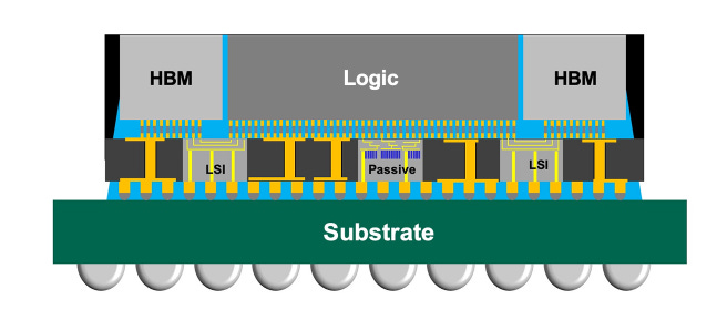
TSMC CoWoS Introduction
However, discrepancies in thermal expansion characteristics among the GPU chips, LSI bridges, RDL interposers, and motherboard substrates lead to structural warping in the packaging, triggering system failures.
Currently, the GB200 chip design poses significant challenges due to its large size and high power consumption. With a single die area of approximately 800–900 mm² and a power range of 400–600 W, GB200 ranks among the largest AI/HPC chips in the industry. Its substantial size stems from the high transistor density per unit area, enabling exceptional performance.
To manage the heat generated by such chips, high-efficiency cooling systems like liquid cooling are necessary. These systems use water cooling plates to transfer heat from the chip through microfluid channels that enable heat exchange between cold and hot water. The key component here is the Cooling Distribution Unit (CDU), which regulates and distributes the coolant flow throughout the system. Working alongside pumps, radiators, heat exchangers, and controllers, the CDU ensures efficient cooling. Additionally, it filters out impurities to prevent clogging or damage to other components.
The CDU directs water through manifolds into the cooling plates. This process is akin to supplying water to every floor of a skyscraper, where sufficient water pressure is required to ensure that cold water reaches even the top levels. However, excessive pressure could lead to leakage, creating a physical limitation.
Why Data Centers Need Liquid Cooling ?
Solutions and Future Directions
To resolve these challenges, Nvidia might need to overhaul the cooling solution entirely or consider alternative approaches such as silicon photonics for data transmission. These measures could alleviate the physical and thermal constraints currently plaguing the Blackwell series.
Source: ASE
Overheating Issues Reported Again for NVIDIA's Blackwell, Frustrating Customers
Overheating Threatens Performance and Design of Nvidia's Groundbreaking Blackwell AI Chips
tspasemiconductor.substack.com
")

