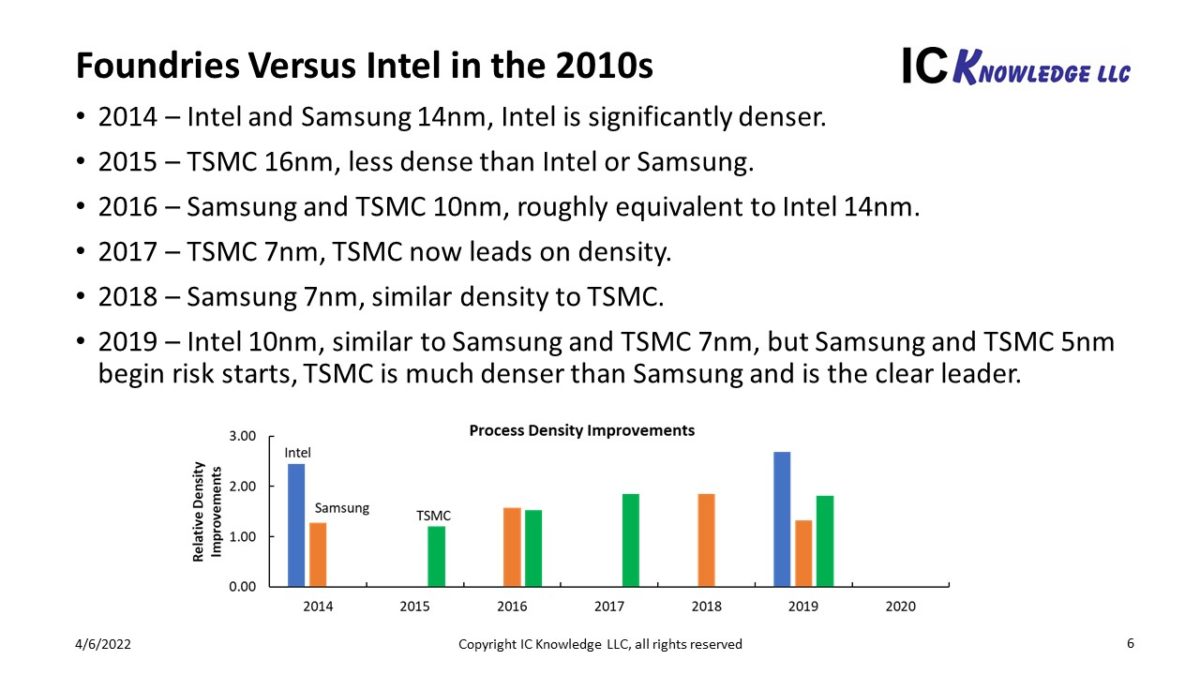
Scott Jones did a nice writeup of this last week:

 semiwiki.com
2024 – in the first half Intel 20A (20 angstrom = 2nm) process is due with a 15% performance improvement. This will be Intel’s first HNS (they call it RibbonFET) and they will also introduce back side power delivery (they call this PowerVia). The backside power delivery addresses IR power drops while making front side interconnect easier. We are estimating a 1.6X density improvement. In the second half of 2024 Intel’s 18A process is due with a 10% performance improvement. We are estimating a 1.06X density improvement making this another half node. This process has been pulled in from 2025 and Intel says they have delivered test devices to customers.
Intel will launch an 18A half node 6 months after 20A? So who is going to design to 20A? As with other half nodes like N7, N7+, and N6, they use the same fab and I expect Intel will do the same. Generally the first node is the biggest N7 versus N6 and N5 versus N4 but I expect the opposite from 20A and 18A. TSMC however spaces their half nodes one year apart versus 6 months. Thoughts?

Can Intel Catch TSMC in 2025? - Semiwiki
At the ISS conference held from April 4th through 6th I presented on who I thought would have the leading logic technology in 2025. The following is a write up of that presentation. ISS was a virtual conference in 2021 and I presented on who currently had logic leadership and declared TSMC the...
2024 – in the first half Intel 20A (20 angstrom = 2nm) process is due with a 15% performance improvement. This will be Intel’s first HNS (they call it RibbonFET) and they will also introduce back side power delivery (they call this PowerVia). The backside power delivery addresses IR power drops while making front side interconnect easier. We are estimating a 1.6X density improvement. In the second half of 2024 Intel’s 18A process is due with a 10% performance improvement. We are estimating a 1.06X density improvement making this another half node. This process has been pulled in from 2025 and Intel says they have delivered test devices to customers.
Intel will launch an 18A half node 6 months after 20A? So who is going to design to 20A? As with other half nodes like N7, N7+, and N6, they use the same fab and I expect Intel will do the same. Generally the first node is the biggest N7 versus N6 and N5 versus N4 but I expect the opposite from 20A and 18A. TSMC however spaces their half nodes one year apart versus 6 months. Thoughts?
