Array
(
    [content] => 
    [params] => Array
        (
            [0] => /forum/threads/cannon-will-they-ever-compete-with-asml.19090/
        )

    [addOns] => Array
        (
            [DL6/MLTP] => 13
            [Hampel/TimeZoneDebug] => 1000070
            [SV/ChangePostDate] => 2010200
            [SemiWiki/Newsletter] => 1000010
            [SemiWiki/WPMenu] => 1000010
            [SemiWiki/XPressExtend] => 1000010
            [ThemeHouse/XLink] => 1000970
            [ThemeHouse/XPress] => 1010570
            [XF] => 2021770
            [XFI] => 1050270
        )

    [wordpress] => /var/www/html
)

Cannon, will they ever compete with ASML?

Arthur Hanson

Well-known member
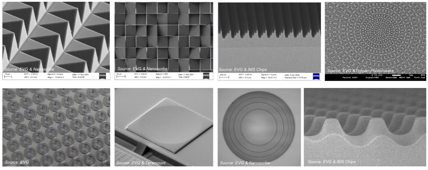
Anhttps://www.anandtech.com/show/21097/canons-nanoimprint-lithography-tool-can-challenge-euv-scannersy

Any thoughts on this new Cannon EUV technology and if it will change any part of the semi world? Will Cannon become a competitor at even the lower end and can this technology advance to the higher end?
 
The biggest problem is that the mechanical force deforms underlaying layers, making it unsuitable for multilayer chips:

The downside comes with alignment on multiple metal layers, which is the main advantage of optical lithography. The process of pressing the mold used in NIL into the resist can cause distortions or deformations, leading to misalignments between the different layers. Leading-edge semiconductors can have more than two dozen layers, each aligned precisely with the layer below to ensure accurate and reliable chip performance. This is especially problematic for advanced semiconductor nodes, where the feature sizes are shrinking below 10nm. Tolerances for overlay alignment at those dimensions is extremely stringent.

“Nanoimprint is the ideal lithography tool for nano-structure definition that does not require alignment, or more accurately does not require many layers of alignment,” says Theodor Nielsen, CEO at NIL Technology.

 
The biggest problem is that the mechanical force deforms underlaying layers, making it unsuitable for multilayer chips:


Canon reported achieving ~2 nm overlay, but they most likely haven't tested the multilayer stacks for cracking etc.
 
The biggest problem is that the mechanical force deforms underlaying layers, making it unsuitable for multilayer chips:


That's a good article. I didn't know this:

"Canon Nanotechnologies is betting big on 3D NAND flash for its NIL manufacturing technology. The company currently has test equipment in place at SK Hynix and in Kioxia’s (formerly Toshiba) fabrication facility and plans to begin mass producing 3D NAND flash using NIL by 2025. Canon also is building a new $357 million factory in Utsunomiya, north of Tokyo, to double the production of its lithography equipment, including NIL"
 
Back
Top