Array
(
    [content] => 
    [params] => Array
        (
            [0] => /forum/threads/asml-high-na-euv-assembly-speeds-up-intel-has-completed-the-second-installation.21188/
        )

    [addOns] => Array
        (
            [DL6/MLTP] => 13
            [Hampel/TimeZoneDebug] => 1000070
            [SV/ChangePostDate] => 2010200
            [SemiWiki/Newsletter] => 1000010
            [SemiWiki/WPMenu] => 1000010
            [SemiWiki/XPressExtend] => 1000010
            [ThemeHouse/XLink] => 1000970
            [ThemeHouse/XPress] => 1010570
            [XF] => 2021770
            [XFI] => 1050270
        )

    [wordpress] => /var/www/html
)

ASML: High NA EUV Assembly Speeds Up, Intel Has Completed the Second Installation

XYang2023

Well-known member
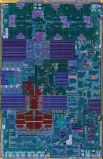
ASML's new CEO, Christophe Fouquet, attended the SPIE conference and delivered a speech focusing on the High NA EUV exposure machine. He also confirmed that Intel's second High NA EUV exposure machine has been assembled.

Christophe Fouquet stated that it is unlikely for the High NA EUV exposure machine to experience delivery delays like the current standard EUV exposure machines. The reason is that ASML has found a new method for assembling scanner sub-components: installing them directly at the customer's factory without the need for disassembly and reassembly. This approach will significantly save time and costs for both ASML and its customers, helping to accelerate the shipment and delivery of High NA EUV exposure machines.

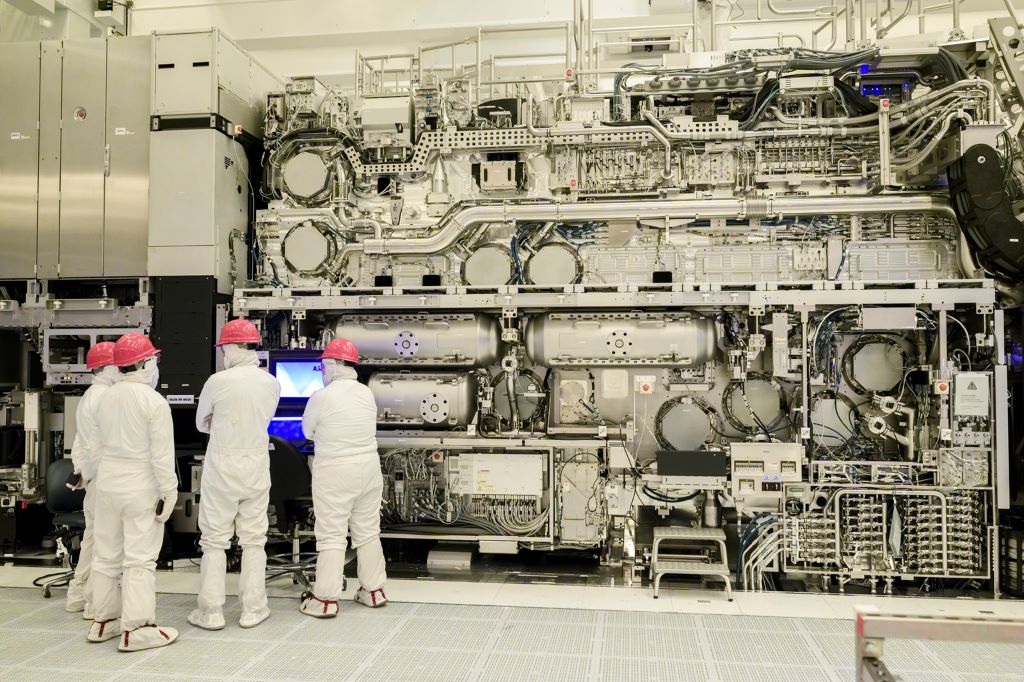
Immediately following Christophe Fouquet was Intel Fellow and Director of Lithography Technology, Mark Phillips. He stated that Intel has completed the installation of two sets of High NA EUV exposure systems at its Portland factory. Moreover, Mark Phillips revealed some data showing that the improvements brought by the High NA EUV exposure machines compared to standard EUV exposure machines might be even greater than previously imagined.

Mark Phillips emphasized that, due to gained experience, the installation speed of the second High NA EUV exposure system was even faster than the first. It is reported that all the necessary infrastructure required for the High NA EUV exposure equipment is already in place and operational. Mask inspection work for High NA EUV exposure has begun as planned. Therefore, Intel can put it into production without much additional support work.

Additionally, Mark Phillips was asked about the issue of CAR (Chemically Amplified Resist) and metal oxide resists. He said that CAR is sufficient for now but may require metal oxide resists at some point in the future. Intel's goal is to have the Intel 14A process technology in mass production in 2026-2027, during which the process technology will be further enhanced.

 
If my memory is correct, intel got first Hi NA EUV in January 2024 and release a video in early March about installation. It seems the installation and qualification time is still around 8-9 months. Looks forward to seeing more Hi NA EUV result reported soon. For mass production, there would be 3-4 more production ready tools needed. It will be quite challenging to shoot on 2026 for HVM. Go for intel and ASML.

 
If my memory is correct, intel got first Hi NA EUV in January 2024 and release a video in early March about installation. It seems the installation and qualification time is still around 8-9 months. Looks forward to seeing more Hi NA EUV result reported soon. For mass production, there would be 3-4 more production ready tools needed. It will be quite challenging to shoot on 2026 for HVM. Go for intel and ASML.


It all depends on how you define HVM. Intel can produce chiplets for internal use from the OR R&D fab but TSMC will have to do millions of SoCs for Apple and QCOM right out of the shute. Different definition of HVM.
 
It all depends on how you define HVM. Intel can produce chiplets for internal use from the OR R&D fab but TSMC will have to do millions of SoCs for Apple and QCOM right out of the shute. Different definition of HVM.
Do they need to wait for the completion of the Ohio site for 14a to accommodate external clients?
 
Do they need to wait for the completion of the Ohio site for 14a to accommodate external clients?

I do know that HNA EUV is a much larger footprint than EUV and requires more power but the Intel OR facility was fitted for one. My guess is that new fabs will need to be built since there will be multiple HNA EUV systems per fab. Ohio sounds about right, in 2-3 years?
 
It all depends on how you define HVM. Intel can produce chiplets for internal use from the OR R&D fab but TSMC will have to do millions of SoCs for Apple and QCOM right out of the shute. Different definition of HVM.
What will you count as a chiplet or not is very vauge For example if 18A die is 110mm2 and apple N3E 18Pro whole SOC die is 8.44*13 109.72mm2 so they are both of the same size Intel yields 500mm2+ chiplet dies in HVM isn't it a bit unfair comparison if we don't account for die size as well in such a case
 

Attachments

  • GZXyo_HasAE8puM.jpg
    GZXyo_HasAE8puM.jpg
    969 KB · Views: 125
What will you count as a chiplet or not is very vauge For example if 18A die is 110mm2 and apple N3E 18Pro whole SOC die is 8.44*13 109.72mm2 so they are both of the same size Intel yields 500mm2+ chiplet dies in HVM isn't it a bit unfair comparison if we don't account for die size as well in such a case

A chiplet is a chiplet, an SoC is an SoC, by definition, two completely different things. Die size is one thing, transistor count (density) is another. The reason why we do chiplets is because they are easier to manufacture than monolithic chips, right? They are easier to design and easier to yield. I think the latest Apple SoC is 20 billions transistors. What is the transistor count on the latest Intel 18A chiplet?
 
It all depends on how you define HVM. Intel can produce chiplets for internal use from the OR R&D fab but TSMC will have to do millions of SoCs for Apple and QCOM right out of the shute. Different definition of HVM.
Could you elaborate on this a bit more. There was some talk about Intel also using standard PDKs and Synopsis / Cadence tools to design chips. They may use internal ip, but is external ip the problem for others? What is the problem that others have with Intel PDK and external tools / ip?
 
The reason why we do chiplets is because they are easier to manufacture than monolithic chips, right? They are easier to design and easier to yield.
Is it a given that chiplets are easier to design? Granite Rapids XCC CPU/compute die (Intel 3) is a "chiplet", but >550mm2. It has some I/O too as it needs to communicate with other chips, and also houses the memory controllers.
 
I do know that HNA EUV is a much larger footprint than EUV and requires more power but the Intel OR facility was fitted for one. My guess is that new fabs will need to be built since there will be multiple HNA EUV systems per fab. Ohio sounds about right, in 2-3 years?
If the standard EUV machine is like the size of a car, the HNA EUV is like the size of a bus.

It is hardly surprising that ASML finds it easier to break it down into components and assemble those on site, instead of building the machine on their premises as a whole unit, disassembling it, and reassembling on the customer site.

This is another reason why they cut down the size of the mask versus having a full mask for High NA. You would need more power, and a much larger laser apparatus, making it even more unwieldy. Maybe the size of a boat.
 
A chiplet is a chiplet, an SoC is an SoC, by definition, two completely different things. Die size is one thing, transistor count (density) is another. The reason why we do chiplets is because they are easier to manufacture than monolithic chips, right? They are easier to design and easier to yield. I think the latest Apple SoC is 20 billions transistors. What is the transistor count on the latest Intel 18A chiplet?
I don't think intel announces Tx Count anymore so that is a something they know

can't i split my SOC to tile/chiplet to save costs it is the ultimate factor that drives chiplet as for Density i believe someone like Scotten Jones will have a better idea
 
If the standard EUV machine is like the size of a car, the HNA EUV is like the size of a bus.

It is hardly surprising that ASML finds it easier to break it down into components and assemble those on site, instead of building the machine on their premises as a whole unit, disassembling it, and reassembling on the customer site.

This is another reason why they cut down the size of the mask versus having a full mask for High NA. You would need more power, and a much larger laser apparatus, making it even more unwieldy. Maybe the size of a boat.

What size mask they use?

Is it not 6x6x250?
 
Is it a given that chiplets are easier to design? Granite Rapids XCC CPU/compute die (Intel 3) is a "chiplet", but >550mm2. It has some I/O too as it needs to communicate with other chips, and also houses the memory controllers.
Chiplets are not easier to design than a block or a set of blocks on a single die. In fact, chiplets make the overall design more complex and difficult. Inter-chiplet communications have less bandwidth and higher latency than on-die communications. And the chiplet strategy might require a new overall design as the product strategy evolves, which is probably going to be more complex than designing a chip with a monolithic die. This will tend to lengthen the design schedule, or at least require larger design teams.

Chiplets have three big advantages I'm aware of. Chiplets allow different blocks of the design to be fabricated with the most appropriate process. What's the most cost-effective process for logic chiplets or cache chiplets may not be the most appropriate or cost-effective for I/O chiplets, and there might be multiple types of I/O chiplets. Obviously, groups of small chiplets are easier to manufacture with a higher yield than monolithic chips with comparable functionality. Finally, though I don't think this market really exists yet, but in the future a lot of people think there will be a market for chiplets which will be analogous to hard IP blocks for monolithic chips, to create more complex SiPs cheaper and faster, and allows a company to focus on its unique value-add.
 
Could you elaborate on this a bit more. There was some talk about Intel also using standard PDKs and Synopsis / Cadence tools to design chips. They may use internal ip, but is external ip the problem for others? What is the problem that others have with Intel PDK and external tools / ip?

Intel did have proprietary tools for design (as did all IDMs) but those were phased out years ago. A good friend of mine was on the Intel place and route team 20 years ago. I would guess it has been at least 10 years since Intel went full commercial. In fact, Intel is Synopsys's biggest customer and has been for a long time. Intel is also a big Cadence customer. I will be at a conference next week, I will ask around to get a better date but I think 10 years is a conservative number.

There is a big difference between a foundry PDK and an IDM PDK. TSMC has been making foundry PDKs for 30 years. Samsung has been at it half that long but still cannot match the quality of TSMC's PDKs. For anyone to expect Intel Foundry PDKs to match the quality of TSMC's PDKs right out of the gate clearly does not understand what a foundry PDK is.
 
Chiplets are not easier to design than a block or a set of blocks on a single die. In fact, chiplets make the overall design more complex and difficult. Inter-chiplet communications have less bandwidth and higher latency than on-die communications. And the chiplet strategy might require a new overall design as the product strategy evolves, which is probably going to be more complex than designing a chip with a monolithic die. This will tend to lengthen the design schedule, or at least require larger design teams.

Chiplets have three big advantages I'm aware of. Chiplets allow different blocks of the design to be fabricated with the most appropriate process. What's the most cost-effective process for logic chiplets or cache chiplets may not be the most appropriate or cost-effective for I/O chiplets, and there might be multiple types of I/O chiplets. Obviously, groups of small chiplets are easier to manufacture with a higher yield than monolithic chips with comparable functionality. Finally, though I don't think this market really exists yet, but in the future a lot of people think there will be a market for chiplets which will be analogous to hard IP blocks for monolithic chips, to create more complex SiPs cheaper and faster, and allows a company to focus on its unique value-add.

I stand corrected. Interconnecting the chiplets is proving to be a significant challenge. Chiplets will also make it possible to use multiple foundries and different processes for a single chip which we have already seen with Intel leading the way. That is a big deal.
 
If the standard EUV machine is like the size of a car, the HNA EUV is like the size of a bus.

It is hardly surprising that ASML finds it easier to break it down into components and assemble those on site, instead of building the machine on their premises as a whole unit, disassembling it, and reassembling on the customer site.

This is another reason why they cut down the size of the mask versus having a full mask for High NA. You would need more power, and a much larger laser apparatus, making it even more unwieldy. Maybe the size of a boat.
The standard EUV isthe size of a bus already!
 
I stand corrected. Interconnecting the chiplets is proving to be a significant challenge. Chiplets will also make it possible to use multiple foundries and different processes for a single chip which we have already seen with Intel leading the way. That is a big deal.
is there any possiblity that Intel generate and release their IDM PDK in incremental way?
 
Back
Top