You are currently viewing SemiWiki as a guest which gives you limited access to the site. To view blog comments and experience other SemiWiki features you must be a registered member. Registration is fast, simple, and absolutely free so please, join our community today!
TechInsights has completed an exploratory teardown and process analysis of the Huawei Kirin 9030 application processor used in the new Mate 80 Pro Max. Our structural and dimensional analysis confirms that the chip is manufactured using SMIC’s N+3 process, a scaled evolution of its 7nm-class technology, and a key indicator of how close SMIC is to achieving a true 5nm-equivalent node without EUV lithography.
Our Kirin 9030 analysis confirms SMIC’s N+3 node and reveals how it compares to industry 5nm. Get process measurements, density benchmarks, and expert analysis.
While SMIC’s N+3 process shows meaningful density improvements, our comparative measurements confirm it remains significantly less scaled than leading commercial 5nm nodes offered by TSMC and Samsung. Full competitive metrics—including gate density comparisons
While SMIC’s N+3 process shows meaningful density improvements, our comparative measurements confirm it remains significantly less scaled than leading commercial 5nm nodes offered by TSMC and Samsung. Full competitive metrics—including gate density comparisons
My objection to TechInsights' or Jukan's spin is that the difference between TSMC's and Samsung's 5nm densities is more than the difference (or ratio) between Samsung and SMIC.
AFAIK Samsung's 5nm node is half node of their 7nm EUV process, and TSMC's is full node from their N7. So if SMIC's density is similar to Samsung's then it's more like 7nm-equivalent process.
Yeah, I remembered the gate pitch had been "abnormally" large, but actually it's just that SMIC density < Samsung density < TSMC density for a given process family or cluster.
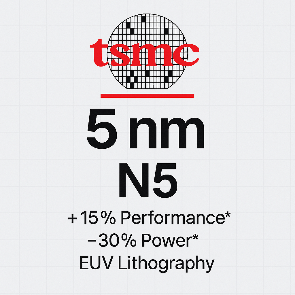
Overview TSMC N5 (5-nanometer process node) is a high-volume FinFET-based semiconductor manufacturing technology developed by Taiwan Semiconductor Manufacturing Company (TSMC). It succeeded the N7 (7nm) family and introduced substantial improvements in performance, power, and transistor density...
Overview TSMC N5 (5-nanometer process node) is a high-volume FinFET-based semiconductor manufacturing technology developed by Taiwan Semiconductor Manufacturing Company (TSMC). It succeeded the N7 (7nm) family and introduced substantial improvements in performance, power, and transistor density...
I used the formula in that article, but actually I applied it wrongly for the 7nm generation nodes since they were double diffusion break. Here is the correction:
Assuming SMIC has the same double vs. single diffusion break difference, N+3 should be more readily associated with the 5nm crowd.
To get away from these layout assumptions, I'd rather use minimum metal half-pitch as the defining feature, as that sets the main patterning difficulty.
Appreciate all the discussion and accurate numbers on minimum pitches and raw maximum cell densities, but without any discussion of routing rules and litho effects on routing rules, the raw density is a bit meaningless. I still remember the whole fracas back at 14nm/16nm, where Intel was claiming a raw library density around 37–45 MTr/mm² but only delivering a density in the mid-teens on Atom, while TSMC was delivering 20 MTr/mm² in the Apple A9, even though they had a far lower raw density. Some of that Intel “loss” is related to chip composition and methodology, but they also had routability issues.
TSMC N6 changed diffusion break from double to single, that in itself is enough to put it above 100 MTr/mm2. So it is a noticeable jump in density from earlier 7nm. The design rules were (supposedly) the same as N7 though I think gate pitch shrunk to 54 nm to get the number below.
I had checked with the author, they may not be using the same ratio of FF:NAND. So absolute numbers may vary from source to source. But within a given author's consistency, the density ratios would be the same and still give the same plot appearance.
 www.techinsights.com