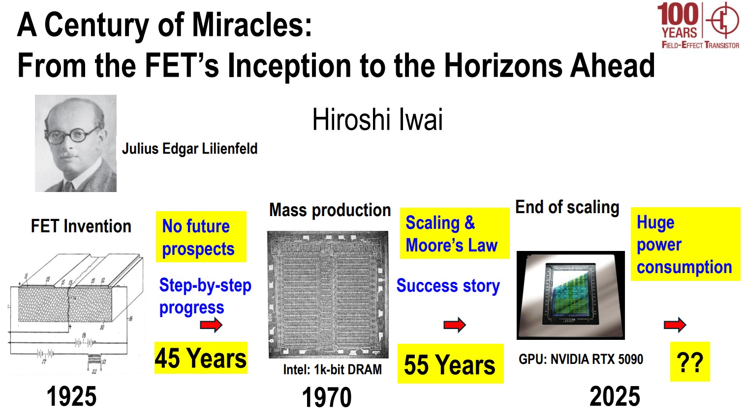


The Field-Effect Transistor (FET), a cornerstone of modern electronics, marks its centennial in 2025, tracing back to Julius Edgar Lilienfeld’s groundbreaking invention in 1925. Born in 1882 in what is now Lviv, Ukraine, Lilienfeld was a prolific physicist who earned his PhD from Berlin University in 1905. His early work at Leipzig University focused on vacuum conduction, contributing to X-ray tubes and even collaborating with Count Ferdinand von Zeppelin on dirigibles. A friend of Albert Einstein, Lilienfeld relocated to the United States in 1927 to defend his X-ray patents, eventually directing research at Ergon Laboratories in Malden, Massachusetts. There, he explored electrolyte interfaces and semiconductors, leading to his FET patents. Retiring to St. Thomas in 1935 due to allergies, he continued research until his death in 1963 at age 81.
Lilienfeld’s FET aimed to replace bulky vacuum tubes, invented in 1906 by Lee De Forest for wireless communication. Vacuum tubes controlled electron beams easily via grid potential in a vacuum. However, semiconductors posed challenges: abundant charges made current control by a gate electrode nearly impossible. Lilienfeld proposed structures like a MESFET in 1925 using p-type semiconductors with Schottky contacts and a MOSFET in 1928 with an aluminum oxide insulator on copper sulfide.
From 1925 to 1960, FET development stalled with a “hopeless period.” Materials like Cu2S and Cu2O were poor choices, semiconductor purity was abysmal, and foundational physics and technologies were lacking. Progress accelerated around 1940 when silicon was refined for military radar detectors, achieving 99.8% purity via thermal processes. This led to Russell Ohl’s accidental discovery of the pn junction in 1940, separating p-type (boron) and n-type (phosphorus) impurities, enabling photovoltaic and rectification effects.
Key theoretical advances followed. In 1938, Walter Schottky described inversion and depletion layers at metal-semiconductor junctions. Heinrich Welker proposed an inversion layer channel in 1945, noting its thinness for easy gate control and low scattering in depletion regions. By 1953, Walter Brown and William Shockley demonstrated FET operation using a back-gate structure on germanium, incorporating pn junctions for source/drain isolation.
The 1947 invention of the point-contact transistor by John Bardeen and Walter Brattain, followed by Shockley’s bipolar junction transistor (BJT) in 1948, shifted focus temporarily. BJTs benefited from 1950s technologies like silicon crystal pulling, impurity doping, photolithography, ion implantation, and epitaxial growth—processes essential for FETs too, but MOSFETs couldn’t be fabricated without them.
Interface instabilities plagued early MOSFETs, with charges like fixed oxide, trapped, mobile ionic, and interface states causing drift until resolved around 1969. This breakthrough enabled mass production of LSIs. Intel’s 1101 256-bit SRAM (1969) and 1103 1k-bit DRAM (1970) featured over 1,000 MOSFETs, using 8-10 µm rules and multiple voltages. The 1971 Intel 4004, the first microprocessor, integrated 2,300 pMOSFETs at 10 µm, designed by Federico Faggin, Masatoshi Shima, and others.
Robert Dennard’s 1974 scaling scheme revolutionized downsizing: reducing dimensions and voltages by factor K (typically 0.7 every 2-3 years) maintained power density while boosting speed and density. Over 25 generations from 1964’s 20 µm to 2025’s 2 nm, this yielded nanoelectronics, transitioning from PMOS/NMOS to CMOS, bulk to FinFET/GAA structures.
By 2025, line widths approach 10 nm limits—practical (demerits outweigh benefits), direct-tunneling (~3 nm), and atomic (~0.3 nm). Memory cells rival influenza virus sizes; chips hold 100 billion transistors, wafers trillions, rivaling galactic stars.
Yet, challenges loom, especially for AI. Semiconductor-based AI systems consume vastly more power than human brains: a massive AI with 5,000 GPUs uses 50 MW for 500 trillion “synapses,” versus a human’s 100 trillion synapses at 100 W. MOSFETs leak subthreshold current even “off,” unlike efficient biological synapses operating at <100 mV and <1 kHz without constant voltage.
Bottom line: This inefficiency explains why nature favors biology over semiconductors for cognition. Future horizons may involve bio-inspired designs or new materials to curb power hunger, ensuring FET miracles continue.
Also Read:
Samtec Ushers in a New Era of High-Speed Connectivity at DesignCon 2026
Silicon Catalyst at the Chiplet Summit: Advancing the Chiplet Economy
Accellera Strengthens Industry Collaboration and Standards Leadership at DVCon U.S. 2026
Share this post via:


Musk’s Orbital Compute Vision: TERAFAB and the End of the Terrestrial Data Center