

At the 2026 Chiplet Summit, Synopsys presented a bold vision for the future of semiconductor innovation: AI-driven multi-die design powered by agentic intelligence. As the semiconductor industry shifts rapidly toward chiplet-based architectures and 3D stacking, the complexity of design, verification, and system integration has increased dramatically. Traditional methodologies, while powerful, are no longer sufficient to keep pace with market demands for higher performance, lower power, faster time to market, and greater reliability. AI is now emerging as the transformative catalyst that re-engineers the entire multi-die design workflow.
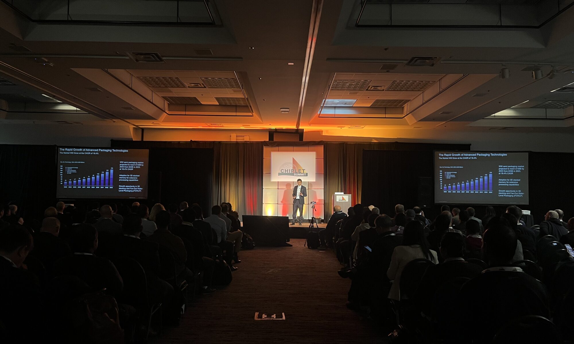
Industry momentum behind chiplets and advanced packaging technologies is accelerating. A significant percentage of design teams are already implementing or planning multi-die architectures in their next-generation products. The global semiconductor packaging market is projected to grow substantially through 2033, fueled by 3D stacking, 2.5D interposers, embedded silicon bridges, and fan-out wafer-level packaging. This growth reflects a fundamental shift: system-level performance gains are increasingly achieved through heterogeneous integration rather than traditional monolithic scaling.
At the same time, artificial intelligence models themselves are driving unprecedented hardware requirements. The evolution from early neural networks like AlexNet to transformer-based architectures such as BERT and large-scale systems like GPT-4 demonstrates exponential growth in parameter counts and computational demand. These AI workloads require advanced multi-die systems capable of delivering massive bandwidth, low latency, and optimized power efficiency. Hardware innovation is therefore both driven by AI and enabled by AI, a powerful feedback loop shaping the next decade of semiconductor design.
However, multi-die design introduces immense multidimensional complexity. Engineers must simultaneously optimize system partitioning, die-to-die connectivity, packaging, power delivery, thermal behavior, signal integrity, verification coverage, and software modeling. Achieving optimal results traditionally requires repeated cycles of tuning tool options, analyzing outputs, and rerunning flows, an iterative search across a vast solution space. Expert engineers rely on years of experience to navigate these trade-offs efficiently.
AI transforms this process by enabling engineering teams to perform like experts at scale. Machine learning models correlate tool settings with performance outcomes, learn the impact of design choices, and guide optimization decisions intelligently. For example, AI-driven die-to-die routing techniques have demonstrated dramatic improvements in runtime and signal integrity. Frequency-domain metrics can accelerate optimization, while time-domain eye-diagram analysis provides higher fidelity insights. By combining these intelligently, AI achieves faster convergence with improved quality of results.
Verification also benefits significantly from AI assistance. Traditional constrained-random approaches often require thousands of test seeds to reach target coverage. AI-assisted verification expands coverage while reducing the number of required tests, achieving faster time-to-results and improved quality-of-results (QoR). This reduction in redundant test iterations directly shortens development cycles and lowers compute costs.
Beyond digital implementation and verification, AI is reimagining multiphysics analysis. Machine learning-enabled solvers accelerate simulation across electrical, thermal, and mechanical domains. Reduced-order models and digital twins enable rapid lifecycle exploration, while generative AI systems assist with scripting, constraint generation, and workflow optimization. These capabilities create predictive, fast, and high-fidelity design environments that were previously unattainable.
One of the most compelling advancements presented is the concept of agentic AI, AI systems that go beyond assistance to autonomous orchestration. Instead of merely suggesting optimizations, agentic AI can plan, act, and make decisions within defined objectives. This evolution moves from simple task execution (L1 assistance) toward full workflow autonomy (L5 decision-making). Engineers increasingly collaborate with AI “co-workers” capable of autonomously partitioning multi-die systems, optimizing power networks, resolving signal integrity violations, and even improving RTL for power and performance.
Industry leaders recognize this shift. My favorite semiconductor CEO Jensen Huang of Nvidia has publicly stated that AI employees will become commonplace, envisioning a future where organizations deploy large numbers of AI-driven engineering agents. This perspective underscores the growing confidence that autonomous AI systems will fundamentally augment, and in some cases transform engineering workflows.
The productivity gains reported by leading CPU, GPU, memory, and hyperscale infrastructure providers reinforce this momentum. Tasks that previously required days can now be completed in hours, or even minutes, through AI assistance. Such improvements are not incremental; they represent a structural change in how semiconductor innovation progresses.
Bottom line: AI-driven multi-die design is not merely about automation, it is about amplification. By combining human expertise with autonomous AI agents, the industry can break through existing performance barriers, reduce time to market, and manage escalating system complexity. As advanced packaging technologies continue to grow and AI workloads expand, agentic AI will become indispensable in shaping the future of semiconductor engineering.
CONTACT SYNOPSYS
Also Read:
Smarter IC Layout Parasitic Analysis
Accelerating Static ESD Simulation for Full-Chip and Multi-Die Designs with Synopsys PathFinder-SC
2026 Outlook with Abhijeet Chakraborty VP, R&D Engineering at Synopsys
Share this post via:


Comments
There are no comments yet.
You must register or log in to view/post comments.