How do most IC design teams organize their work during the design process?
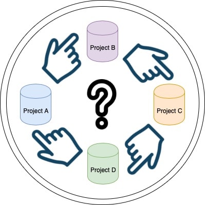
Most design teams would say that they organize their work into a project-centric view, and that at the beginning of the process use a tool for requirements management, maybe a bug tracker, or some design management tool. On the four IC designs that I worked on in the 70’s and 80’s, each one took a project-centric view, and there was virtually zero IP reuse going on.
Let’s take a closer look at some common issues that arise with a project-centric approach to SoC design.
Scalability
A team starts out on a new SoC and then someone in the CAD groups sets up a new project in each of their tools, like:
- Requirements management
- Bug tracking
- Design Management
Most electronic products tend to reuse cells, blocks, modules and sub-systems from previous products, but how does a project-centric flow account for any of this IP reuse?
Any dependencies in these IP blocks are not really handled with point tools that basically silo design data. Each new project then gets a new DM server instance, and who is going to maintain these servers for years or even decades?
If your company has four concurrent projects going on, then who is tracking what is commonly used between each of the projects, when all of the tools are setup per project?
If your tools only understand the scope of what’s inside each Project, then there’s a gap of knowing what happens if a common cell, block, module or sub-system (IP) is changed or a bug is fixed, creating a new version.
Collaboration
Common IP blocks being used within multiple projects makes collaborating a challenge, because each project has their own permission settings, as individual servers are setup per project. Who wants to stop an ongoing project to request access to all IP blocks being used?
Traceability
When purchasing design or verification IP you have to sign a license agreement with each vendor, and these vendors want to track how many instances of their valuable IP is being used to ensure that the agreement terms are being met. You really want to know how all IP is being used, across all projects, not just within one project.
Countries have laws in place regarding how silicon IP is being used or exported, and for American companies the U.S. Department of State has defined the International Traffic in Arms Regulations (ITAR). Your company needs to know how each IP block complies with ITAR or other local requirements.
If a bug is found inside some IP block, and that block is re-used in multiple projects, then how does each project team hear about the bug fix?
IP-centric Design Process
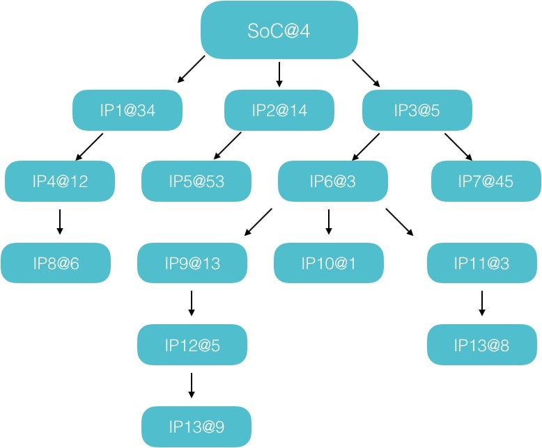
There is an alternative approach to a project-centric design process with its challenges, and that is to use an IP-centric design process. Instead of each project being a silo of design data, each project can be treated as an IP block as part of a connected hierarchy of other IP blocks as shown below:
With this IP-centric approach each Project continues to have its own permissions and DM backend as desired. IP metadata goes along with each IP block, so that all users of an IP block have all the info they need when reusing. Even dependencies from bug tracking tools and requirements tools are integrated into this IP-centric view.
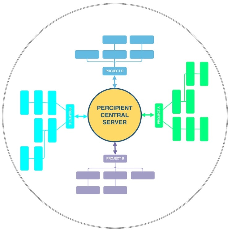
Scaling works well because there’s a centralized server that can be quickly update once there’s an IP update, then its effects are seen in all projects. This is the approach that Methodics has taken with Percipient, their IP Lifecycle Management (IPLM) tool. Shown below are four projects being managed with the Percipient central server.
Your company can even follow a Zero-Downtime upgrade policy while using a central server approach.
When a bug is found for an IP block in Project A, then an engineer would file a bug report under Project A. Engineers on Project B and C would then note that a new bug was just filed on the re-used IP block.
Summary
Times have changed, and IC designs are getting larger every day, so the approach that your company and teams take makes a difference. The project-centric approach worked OK for small designs with little IP reuse, however for today’s SoC projects you’d be better served with the IP-centric approach being offered by Methodics. I like how they’ve integrated with other bug tracking and DM tools, so you don’t have to ask your CAD group to customize lots of point tools to play well together.
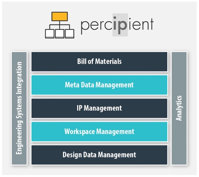
Here’s a final view of how Percipient provides several useful management features.
To read the complete 10 page White Paper, browse here.
Related Blogs
- Avoiding Fines for Semiconductor IP Leakage
- Webinar Recap: IP Security Threats in your SoC
- Workflow Automation Applied to IP Lifecycle Management
- Achieving Functional Safety through a Certified Flow


Musk’s Orbital Compute Vision: TERAFAB and the End of the Terrestrial Data Center