
LUBIS EDA is a Germany-based EDA company that specializes in formal verification, a mathematically rigorous method for proving that a chip design behaves correctly under all possible conditions. Founded in 2021 by a team of researchers and engineers from the academic world, the company has rapidly become a notable innovator in an area that the semiconductor industry increasingly recognizes as mission-critical.

The Problem: Verification Is the Modern Bottleneck
In contemporary microchip development and verification the process of ensuring that hardware behaves as intended is widely understood to be the most time-consuming and risk-laden part of the design flow. Traditional simulation-based methods use constrained random test benches to exercise portions of a design, but they can miss “corner cases” rarely triggered interactions that nonetheless can cause functional failures on silicon. As chip complexity scales with AI, high-performance computing, and automotive systems, the number of possible states a design can enter grows exponentially, overwhelming traditional simulation approaches and leading to costly tape-out errors or respins.
Formal verification, in contrast, mathematically proves properties of a design, such as protocol compliance, safety conditions, or correctness of state transitions across all possible inputs and states. This exhaustive nature allows it to find bugs that simulation might never trigger, particularly in deep corner-case scenarios. However, formal verification has historically been difficult to scale and integrate into standard workflows because it relies on manually written assertions and specialized expertise.
LUBIS EDA’s Approach: Automating Formal Verification
LUBIS EDA’s core offering tackles this gap with a blend of software tools, automation frameworks, and consulting services designed to make formal verification more practical, scalable, and integrated with modern chip design flows:
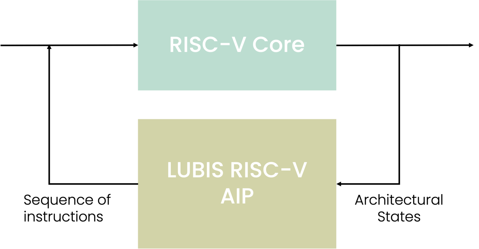
Automated Assertion Generation: One of the biggest barriers to formal verification is writing correct, reusable assertions (properties) that explain what the design should do. LUBIS’s platform automates much of this work by generating Assertion IP based on models and reusable patterns rather than requiring handcrafted properties for each block.
Formal-Ready Verification Environments: The company advocates not just using a tool, but creating a formal-ready environment where assertion libraries, scenario controls, and CI-integrated workflows allow formal tools to be used routinely alongside simulation. This integrated environment improves coverage visibility, reuse of verification assets, and regression tracking across design projects.
Cloud-Based EDA Solutions
LUBIS offers a cloud-hosted version of its tools “LUBIS-on-cloud” that requires no local installation, enabling teams to scale formal verification across multiple designs and pipelines with minimal setup overhead.
Consulting and Training Support: Recognizing that formal verification is still specialized, LUBIS EDA also provides expert consulting, including turnkey formal sign-off services, custom verification engagements, and training helping teams adopt best practices and resolve problems that simulation alone cannot.
Collectively, this combination positions LUBIS not merely as a tool vendor but as a workflow provider that bridges simulation and formal verification in a way that modern teams can operationalize.
Real-World Impact
Evidence of the effectiveness of formal methods, and by extension the value of LUBIS’s solutions, comes from documented case studies where formal verification led to the discovery of bugs that simulation had missed entirely. For example, formal flows have uncovered issues in pipelined RISC-V cores and standard protocols that could have caused functional failures in silicon, demonstrating that formal techniques catch errors early and reduce the risk of expensive respins or delays.
Why This Matters Now
The semiconductor industry’s challenge is not just designing complex chips, it’s ensuring correctness under all conditions while meeting aggressive time-to-market targets. Verification accounts for a disproportionately large share of design effort and cost, and failures at this stage can incur extraordinary financial damage. LUBIS EDA’s strategy, automation, integration, and formal rigor, directly addresses this fundamental industry pain point, potentially shifting verification from a bottleneck into a predictable, measurable phase of development.
Bottom line: As chip designs continue to get more complex and safety-critical especially in AI accelerators, autonomous systems, and edge computing demand for automated, scalable formal verification is likely to grow. LUBIS EDA’s tools and methodologies, focused on reducing human effort and increasing coverage confidence, align with this trend. Their model of combining software with consulting and training encapsulates a broader transformation in EDA: tools no longer just exist in isolation but become part of an automated, data-driven verification ecosystem.
Also Read:
Assertion-First Hardware Design and Formal Verification Services
Assertion IP (AIP) for Improved Design Verification
Automating Formal Verification
CEO Interview: Tobias Ludwig of LUBIS EDA
Share this post via:


Comments
There are no comments yet.
You must register or log in to view/post comments.