![SILVACO 051525 Webinar 400x400 v2[62]](https://semiwiki.com/wp-content/uploads/2025/04/SILVACO_051525_Webinar_400x400_v262.jpg)

I’ve read articles about power electronics, RF systems and high-frequency applications using SiC and GaN transistors, especially in EVs and chargers, but hadn’t looked into the details of GaN devices. A recent Silvaco webinar proved to be just the format that I needed to learn more about GaN design and optimization. Udita Mittal, Field Application Engineer at Silvaco presented this webinar aimed at process engineers, simulation engineers and fabrication engineers.
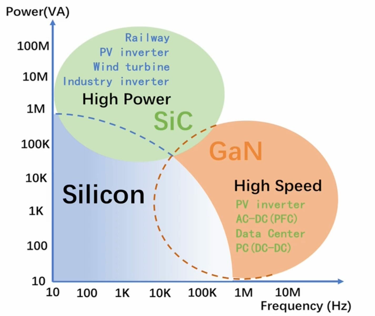
GaN and SiC devices provide a wide bandgap, high electron velocity and high temperature range, making them ideal for power electronics applications. Here’s where Silicon, SiC and GaN technologies are being used across the power and frequency spectrums.
The first type of GaN device introduced in detail was a GaN HEMT (High Electron Mobility Transistor) dubbed a pGaN, where the cross-section is shown below:

The pGaN has a high sheet carrier density at the red-dashed interface, caused by the unique polarization-induced electric field. TCAD tools accurately model the Schottky gate, alGaN barrier, high electric fields, SiN passivation and the buffer layer. Many parameters impact the device performance, like: polarization charge, bulk traps, interface traps, metal workfunction, electron/hole mobility along the interface and the substrate stack. The good news is that Silvaco has many TCAD and EDA tools to accurately design and optimize GaN devices:

Process simulation is driven by the physics, where the GDSII layouts create each process layer, etching and deposition are modeled, implantation is simulated, and even stress and strain effects from the local lattice mismatch and thermal mismatch are calculated. Here’s the GaN mobility model produced with velocity saturation effects

The Victory DoE tool is both a project manager and DoE tool, while Victory Analytics provides analytics along with machine learning. You provide the desired targets, then Victory Analytics feeds back the input values to achieve the targets. This approach gives insight about which parameters are dominant.
Udita presented the fabrication flow for a normally off GaN HEMT to optimize the device structure and electrical performance. Users can then visualize the process cross-section and device characteristics.

Using TCAD, the key inputs were identified that affected steady state IV characteristics. A DoE analysis showed how IdVd was impacted by the AlGaN barrier thickness and Al mole fraction in AlGaN barrier. Even the breakdown voltage can be modeled in lateral HEMTs.
The final device example discussed was a vertical GaN (CAVET), where Victory Process and Victory Device were used to create IV curves, dominant model parameters were selected with Victory Analytics, and sensitivity analysis performed in Victory DoE. Victory Analytics also generated a ML regression model and visualized FoM (Figure of Merit) trends.
Creating SPICE models from TCAD tools is accomplished with UtmostIV, then simulated with SmartSpice. Utmost creates CMC standard GaN FET models or third-party models.

Summary
Silvaco had broadened its offerings to include TCAD, EDA and Semiconductor IP. The growing demand for power electronics is being met with GaN devices. Using TCAD tools an engineering team can now design and optimize their GaN devices, resulting in faster time to market and improved performance. Victory Design of Experiments and Victory Analysis tools make it possible to explore the design space on the path to an optimized transistor structure modeled as a digital twin.
Customers like ST Microelectronics, Wavetek and Fraunhofer ISIT have used Silvaco tools in their GaN device projects for DTCO.
View the archived webinar online.
Related Blogs
- Simulating Gate-All-Around (GAA) Devices at the Atomic Level
- Silvaco: Navigating Growth and Transitions in Semiconductor Design
- Analysis and Exploration of Parasitic Effects
- Accelerating IC Design: Silvaco’s Jivaro Parasitic Reduction Tool
- Silvaco’s Diffusion of Innovation: Ecosystem Investments Driving Semiconductor Advancements
- Silvaco at the 2025 Design Automation Conference #62DAC
- TCAD for 3D Silicon Simulation


Comments
There are no comments yet.
You must register or log in to view/post comments.