Todd Burkholder and Andras Vass-Varnai, Siemens EDA
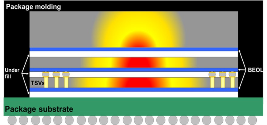
As semiconductor devices become smaller, more powerful and more densely integrated, thermal management has shifted from an afterthought to a central challenge in modern IC design. In contemporary 3D IC architectures—where multiple chiplets are stacked and closely arrayed—power densities reach extreme levels comparable to the surface of the Sun. This is not mere analogy but a demonstrable engineering constraint that defines the boundaries of viable designs today. Consequently, the traditional approach—where thermal analysis was conducted at the end of the design process by esoteric and isolated specialists—is no longer sufficient.
Historically, silicon, package, and system teams worked in silos, with thermal analysis relegated to rule-of-thumb calculations or late-stage verification. In the context of 3D ICs, such practices are a recipe for risk, rework, and likely disaster. With multiple interacting thermal domains in extremely compact spaces, proactive and continuous thermal management is essential from the earliest design phases.
Organizations like Siemens are responding by laying the groundwork for robust thermal analysis workflows that are accessible for design engineers at all skill levels, and that are no longer confined to dedicated thermal analysts possessing esoteric knowledge.
The thermal analysis 3D IC conundrum
Thermal models are foundational for advanced IC packaging. Accurate modeling determines not just whether a chip will function, but also how long it will last and how reliably it will operate. Overheating or poorly managed thermal gradients can corrupt data, degrade performance or cause premature field failures—outcomes with both technical and business consequences.

This risk is especially pronounced in heterogeneous 3D IC stacks, where devices with different thermal tolerances are integrated together. For instance, high-power logic may safely reach junction temperatures above 110°C, but adjacent high-bandwidth memory may need to operate below 90°C to retain data integrity. Tight proximity optimizes data transfer and electrical performance, but it also creates substantial risk of cross-heating. If a thermal problem is not identified until after layout, required changes can be staggeringly expensive and time-consuming.
Effective 3D IC thermal analysis is not just about improved simulation. It demands unified workflows and seamless communication across electrical, mechanical, and system domains. One of the most pervasive challenges in the industry is the lack of common tools, culture, and terminology. Silicon designers, package architects, and thermal analysts often operate in their own environments, with minimal cross-team or cross-domain data exchange.
This fragmented structure complicates the creation and updating of accurate thermal models. Constructing reliable models often requires detailed physical characterization of chiplets, interposers, substrates and interconnects. The level of necessary detail can range from broad estimates in early exploration to intricate sign-off models. Unfortunately, most models are built manually—and typically late in the process. As a result, any design changes near tape-out can force costly and time-consuming recalibration that is simply unsustainable when each revision can cost millions.
Further adding to the challenge is the disconnect between electrical and thermal disciplines. Electrical engineers may lack insight into thermal issues, while thermal specialists may not grasp silicon constraints. Few current workflows synchronize thermal models automatically as design updates occur, making agile, accurate simulation across the design cycle difficult.
Shift-left thermal analysis
The most effective 3D IC thermal workflow must follow an integrated, dynamic process that begins early in the design phase and continues to keep thermal models current as a design evolves. Shifting thermal analysis “left” means incorporating it much earlier—and updating it continuously—throughout design. This empowers chip designers, package architects, and thermal specialists to work from a consistent, data-rich foundation.
In practice, this translates into updating the thermal model with each design iteration, so that the digital twin always reflects the latest changes. An ideal ecosystem allows all stakeholders to use interconnected tools for seamless data exchange, minimizing manual conversion or handoffs. Under this flow, design, verification and sign-off are not sequential checkpoints but interconnected phases in a fluid, evolving design process.
Key segments are already adopting this approach. Automotive electronics, particularly in AV and ADAS, require chiplet-based designs cooled at the system level. Data center architectures—supporting AI and high-compute workloads—depend on packages with stacked chips and must be analyzed from the die all the way to the system, often including advanced cooling solutions. Efficient bidirectional feedback and holistic analysis are quickly becoming competitive imperatives in these domains.
The democratization of thermal analysis
Democratizing thermal analysis—making it accessible to all engineering disciplines regardless of expertise—is essential for next-generation IC packaging. Recognizing this dire need, Siemens has spent years developing, ground proving, and refining a thermal analysis flow applicable to traditional ICs, SoCs, and 3D ICs.

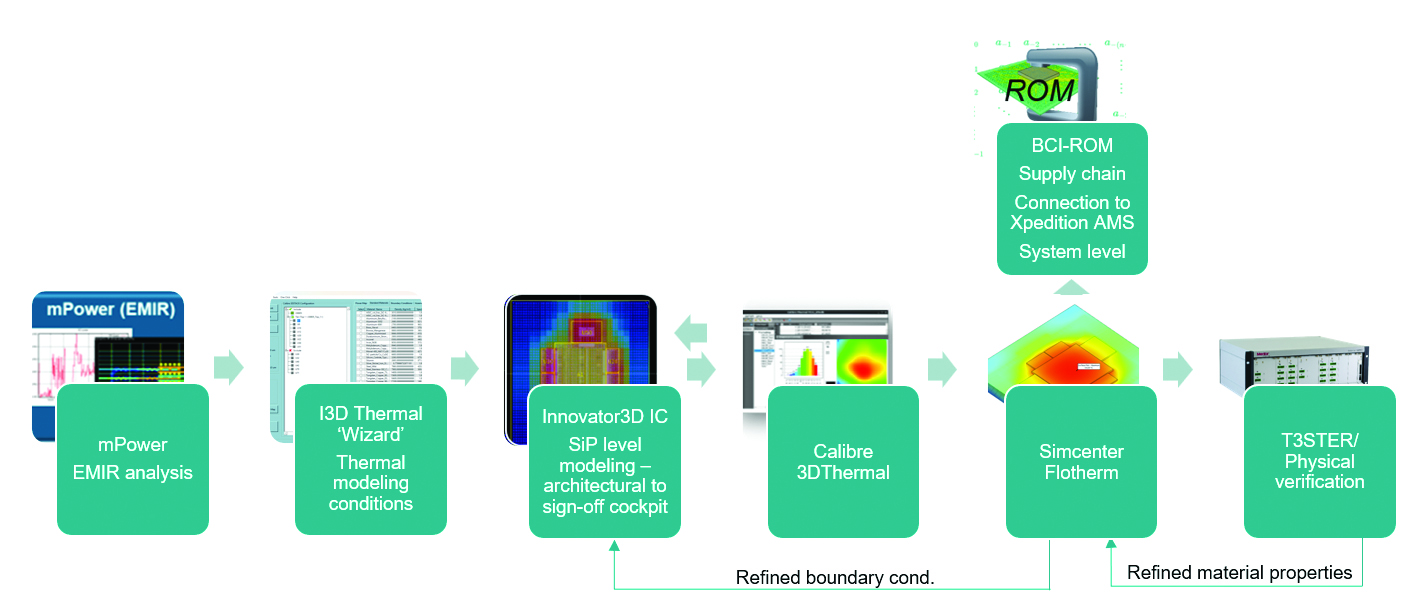
Siemens’ Calibre 3DThermal embodies this philosophy by delivering a unified platform that combines established IC verification with advanced thermal modeling. Calibre 3DThermal converts native IC databases into high-fidelity thermal models and supports designers, including non-specialists, in conducting meaningful simulations and interpreting results.
Package architects benefit as well, using tools like Innovator 3D IC, a unified cockpit for design planning, prototyping, and predictive analysis of 2.5/3D heterogeneous integrated devices. Innovator 3D IC works with Calibre 3DThermal to translate full connectivity data into robust thermal models. This integration enables electrical and thermal verification to advance in step, ensuring design changes propagate efficiently across all domains.
Mechanical engineers leveraging Simcenter Flotherm experience new efficiency as system-level models can now be automatically generated upstream, eliminating redundant rebuilding. This digital continuity ensures a synchronized and accelerated workflow from early silicon through package and system validation.
End users of 3D ICs, in turn, depend on thorough thermal analysis to ensure long-term component reliability. Many now request digital twins of a device’s thermal profile for validation in their application environment. However, sharing detailed thermal models raises IP protection concerns—these models can reveal die sizes, placement, and power distribution. This underscores the need for useful, thermal representations that protect valuable IP.
Siemens has addressed this challenge through Flotherm’s boundary condition independent reduced order models (BCI-ROM). BCI-ROMs preserve the essential thermal profile while safeguarding sensitive structural details, enabling secure collaboration and model sharing throughout the supply chain.
Keeping cool in the third dimension
The future of 3D IC thermal analysis will be shaped by four interconnected trends: greater integration as thermal simulation becomes routine; automation as model updates accelerate; collaboration as teams communicate seamlessly across domains; and democratization as powerful analysis becomes accessible to all contributors. Embracing these trends will enable the semiconductor industry to address mounting thermal complexities while reducing project risk and time-to-market for next-generation applications.
As 3D IC packaging matures, thermal analysis must remain central in order to deliver robust, manufacturable products. The Siemens integrated and automated approach—connecting design roles, automating model creation, and ensuring IP security—sets a compelling example for the industry.
Todd Burkholder is a Senior Editor at Siemens DISW. For over 25 years, he has worked as editor, author, and ghost writer with internal and external customers to create print and digital content across a broad range of EDA technologies. Todd began his career in marketing for high-technology and other industries in 1992 after earning a Bachelor of Science at Portland State University and a Master of Science degree from the University of Arizona.
Andras Vass-Varnai obtained his MSc and PhD degrees in Electrical Engineering from the Budapest University of Technology and Economics. He spent over a decade at Mentor Graphics as a product manager, leading various R&D projects focused on thermal test hardware and methodologies. Before assuming his current role as a 3D IC reliability solution engineer, Andras served as a business development lead in South Korea and the United States. Now based in Chicago, IL, he is dedicated to contributing to the development of a novel 3D IC package toolchain, leveraging his experience in thermal and reliability engineering.
Also Read:
Software-defined Systems at #62DAC
DAC TechTalk – A Siemens and NVIDIA Perspective on Unlocking the Power of AI in EDA
Digital Implementation and AI at #62DAC
Share this post via:


Comments
There are no comments yet.
You must register or log in to view/post comments.