What is Applied Materials doing in an EDA trade show?
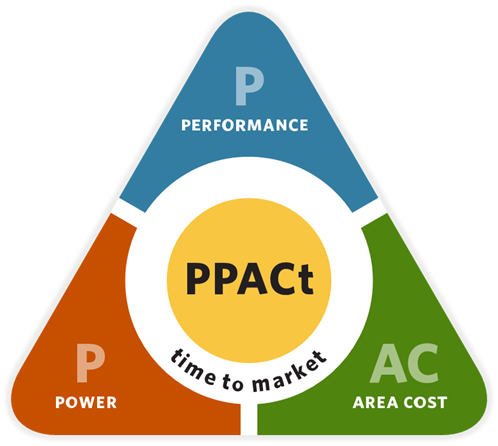
New semiconductor market segments such as AI, automotive and connected devices are growing at an accelerated pace and placing constant increased pressures on the PPAC (power, performance, area, cost) system requirements. In the past, these growing PPAC demands were addressed by scaling down feature geometries and cost per transistor at a predictable pace, known as Moore’s law. But in recent years, geometry scaling has slowed down around 7nm technology geometry to a point that it cannot keep up with the pace of growing PPAC demands, requiring new approaches and innovations.
Today’s technologies are already at atomic levels and there is no single technology breakthrough we can rely on. We need to explore multiple innovative solutions across the entire semiconductor technology chain and holistically evaluate from the system level, chip design architecture, IP design and circuit design, devices, and interconnect to the fabrication processes and materials that this entire chain is founded upon.
PPAC à PPACt
Applied Materials has already identified these challenges a few years ago and has implemented a corporate-wide effort to address them in an integrative manner that explores potential innovative solutions at different levels. Solutions include new material innovations, processing techniques, new device structures, power delivery schemes, interconnect structures, circuit, foundation IP, chip design, and packaging, all the way to the system level. Multiple combinations of these innovations can be modeled and evaluated at each level. Applied’s goal in this effort is to find and develop new solutions with optimized PPAC for each market segment or application. Furthermore, Applied recognizes the importance of bringing these solutions to the market quickly and added a time-to-market dimension changing PPAC to PPACt.

System To Materials (STM) Group
The STM group at Applied is an essential part of this corporate-wide effort. STM has developed technologies and methodologies to identify system level challenges and bottlenecks through innovative solutions at all levels of the value chain. These innovations are accurately modeled through a complete design flow from materials to system level.
STM DAC Exhibit
STM engagements with the design and EDA community are important to understand and address the current industry challenges. At 2024 DAC, learn about the following products and services that are commercially offered by STM at exhibit booth #1522 (under “Sage Design Automation” which is a part of the STM group).
SLiCTM: Standardcell Library Compiler
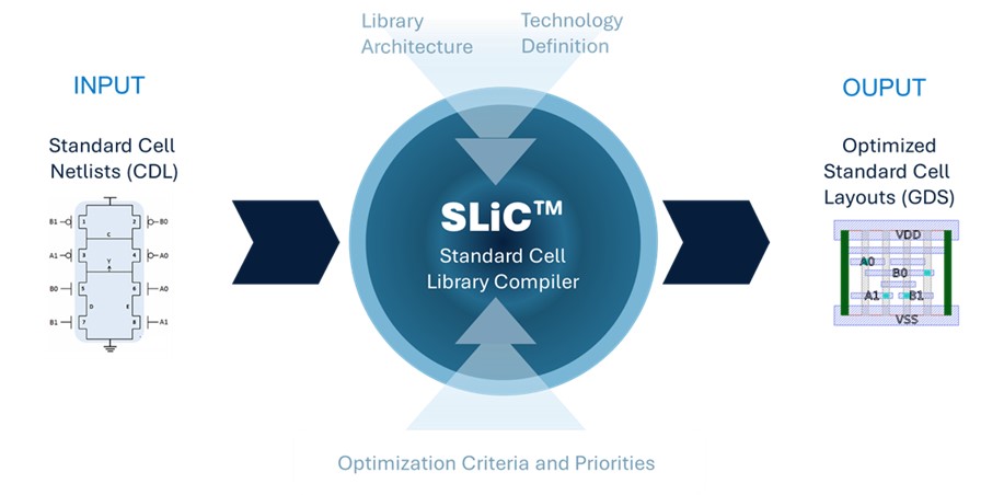
SLiC generates the highest quality standard cells at a fraction of time and effort compared to traditional methods. SLiC’s technology flexibility and quick setup time can accelerate DTCO pathfinding effort from months to weeks. SLiC high throughput and optimized results enable generation of a complete production level logic library overnight. SLiC supports state of the art technologies from 7nm to 1.4nm, including CFET stacked devices.

iDRMTM: integrated Design Rule Management system
iDRM is a tool to develop, manage and enable correct-by-construction design rule development with clear rule description and automate creation of error-free DRC decks for third party DRC tools. iDRM’s powerful GUI helps to view and edit design rules, as well as check and verify design rule intent.
DRVerifyTM: DRC Deck QA and Verification
DRVerify checks and verifies DRC decks to make sure they are complete, correct and error-free. DRVerify automatically creates pass/fail test cases from design rule descriptions, runs the tested DRC deck on these test cases, scans DRC markers, compares to the golden rule intent and highlights any possible errors or mismatch.
Ginestra®: Materials-to-Device Optimizer
Ginestra is a material centric simulation platform which links process material properties (composition, stoichiometry, atomic-defects) to device performances and reliability. Ginestra integrates relevant physics critical to understanding and managing the complexity of materials-to-device co-optimization from materials discovery through device performance, reliability and variability projection. Ginestra’s design and simulation platform accelerates materials-to-device innovation, providing atomic level insights to improve performance, power, area, cost and time to market.
Also Read:
Ansys and NVIDIA Collaboration Will Be On Display at DAC 2024
Arteris at the 2024 Design Automation Conference
EasyLogic at the 2024 Design Automation Conference
S2C Prototyping Solutions at the 2024 Design Automation Conference
Share this post via:


Musk’s Orbital Compute Vision: TERAFAB and the End of the Terrestrial Data Center