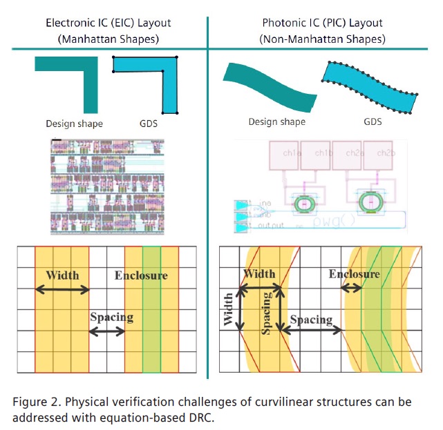
Silicon photonics is getting a lot of interest because it can be used in many applications to improve bandwidth, reduce power and provide novel new functionality. It is especially interesting because it offers an ability to combine electronics and optical elements into the same die. Though it is fabricated with familiar silicon processes and techniques, it is a very different animal when it comes to design automation and verification. In a recent white paper Siemens EDA opines that if methods similar to those used for Electronic Integrated Circuits (EIC) can be applied to the design and verification of Photonic Integrated Circuits (PIC) that there could be explosive growth in their development and use.
The white paper titled “Advancing silicon photonics physical verification through innovation” cites how the development of process design kits and EDA tools allowed the exciting growth we have seen in semiconductors in the last few decades. With silicon photonics it makes sense to follow a parallel path to expand their use. The authors make the point that we are definitely in the early stages of developing complete flows for PICs. However, important first steps have been taken, despite the challenges. PICs do not follow some of the foundational assumptions that work for EICs to help enable software tool development.
The authors focus on PIC verification to make their point. While equivalents to LVS, DRC and DFM are needed, the existing EIC tools cannot be directly applied without specific modifications and adaptations. There are several examples of this. Because CMP is still used there is a need for fill. Yet if traditional square fill shapes are used, they can affect waveguides. PICs require circular fill shapes to avoid these issues. Fortunately, Calibre YieldEnhancer has features in its SmartFill Tool that effectively deal with these new requirements around waveguides. This is just the tip of the iceberg.

The Siemens EDA white paper has a section that discusses how DRC needs to work in PICs. PIC based devices tend to be curvilinear. Piecewise linear approximations used by traditional DRCs lead to inaccuracies. The Calibre nmPlatform supports equation-based DRC that is used to apply complex checks that make allowances to eliminate false errors. The one catch is that this requires modifying the foundry rule deck. To avoid this Siemens introduced a methodology that hands off traditional DRC violations to an Auto-Waiver processing step that differentiates true errors from false errors. The result is that designers can get accurate results within a single nmDRC run.
Another important area is circuit verification. Siemens notes that PIC components are not natively recognized. Each photonic component is essentially a custom device, which prevents recognition and the use of device parameter extraction. Indeed, waveguides are analogous to wires found in EICs, but their behavior and importance are completely dissimilar. The white paper provides several examples of the departures in device interpretation in PICs. Further compounding verification difficulties is that there are often no corresponding schematics for PICs.
Siemens has explored interesting ways to validate PIC devices. They mention one approach where the device being verified is re-rendered and then compared to the on-chip geometry. This requires the use of advanced pattern recognition algorithms. This is clearly an area that is under development, yet where we can expect to see more innovations.
The Siemens white paper offers a valuable discussion of this new area of design automation. As increasing PIC automation is developed, the use of photonics in ICs will grow, bringing their benefits to larger markets. The two flows, EIC and PIC will remain distinct, but may someday reach parity in terms of ease of design. The Siemens white paper offers an interesting glimpse into what is available today and what lies ahead.
Also Read:
Formal Verification Approach Continues to Grow
Transistor-Level Static Checking for Better Performance and Reliability
Embedded Analytics Becoming Essential
Share this post via:


Comments
There are no comments yet.
You must register or log in to view/post comments.