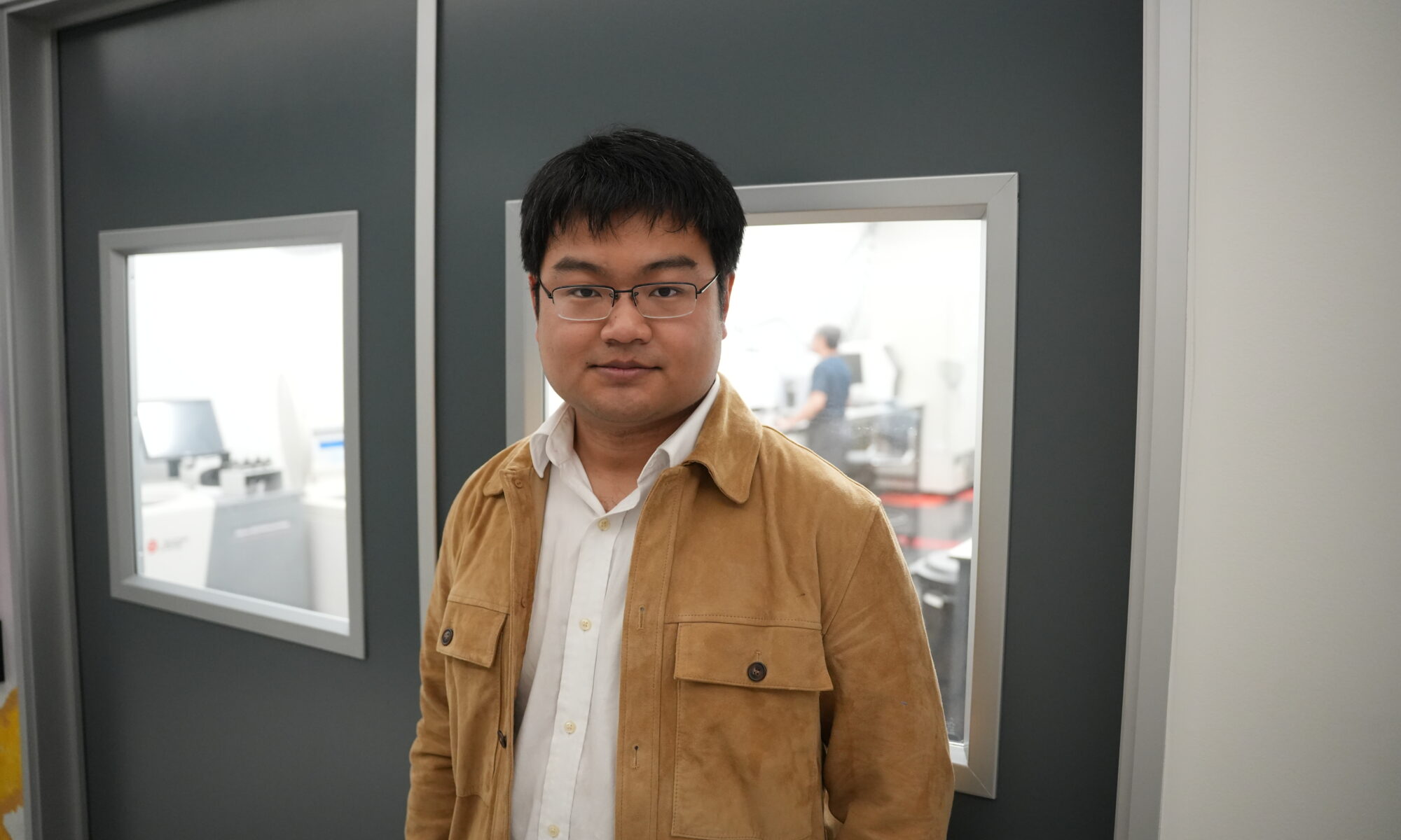
Jiadi Zhu is the CEO and founder of CDimension, a company rethinking chip design to shape the next generation of computing. Under his leadership, CDimension is creating the next generation of building blocks for chips, starting with materials and scaling up to full systems that can power everything from today’s AI and advanced computing to the quantum breakthroughs of tomorrow.
With a Ph.D. in Electrical Engineering from MIT and over a decade of work at the frontier of 2D materials and 3D integration, Jiadi has been widely recognized for his originality in device design and novel semiconductor materials. His research has been published in top journals like Nature Nanotechnology and presented at leading conferences including IEEE’s International Electron Devices Meeting.
Tell us about your company?
CDimension is pioneering a bottom-up strategy for the future of computing, beginning at the foundation of the chip stack: materials. We develop and supply next-generation two-dimensional (2D) semiconductors and insulators, enabling breakthroughs in both semiconductor circuits and quantum computing.
On the semiconductor side, our atomically thin 2D semiconductors significantly reduce power consumption and help overcome the global power wall in computing. On the quantum side, our single-crystalline 2D materials reduce noise at the source,enabling longer coherence times, higher fidelities, and scalable integration of quantum qubits.
Backed by more than 20 patents and a growing base of industrial and academic customers, our roadmap delivers wafer-scale materials today and pilot-scale quantum chips within 18 months. With this foundation, CDimension is positioned as the chip provider of the quantum era, building the material and device layer that will power tomorrow’s computing revolution.
What problem is CDimension solving?
The core issue we are addressing is that silicon has hit its limits. Put simply, chips are getting more power-hungry and harder to integrate. Most of the industry’s fixes we’ve seen up to now are top-down, things like reconfiguring GPUs; but those only deliver incremental gains, not the 100x or even 1000× leap future applications in AI and quantum will require over the next decade.
That’s why we believe the solution has to start at the bottom, with the materials themselves. For decades, 2D materials were stuck in the lab as tiny flakes with high defects and no scalability. We’ve broken that barrier by producing wafer-scale, high-quality semiconductors and insulators that customers can actually build on today.
I like to think of it this way: trying to build the future of chips with silicon alone is like trying to make a book out of bricks. It worked for a long time, but now the bricks are too bulky to stack any further. Our 2D materials are like pages: ultra-thin, smooth, and stackable. From there, you can build the books, or integrated circuits, and eventually even the writing inside, which is applications like quantum computing.
What application areas are your strongest?
Currently, our technology is making the biggest difference in quantum. While the field is gaining momentum, progress has been stalled by one critical bottleneck: noise. These random disturbances cause errors that prevent systems from scaling. Existing approaches struggle to fix it because they rely on imperfect materials or lack robustness at the materials level.
Our wafer-scale, single-crystalline 2D insulators reduce noise at the source. Instead of trying to scale by simply adding more qubits, we’re improving each individual qubit by lowering noise and extending coherence time. That allows more qubits to be connected reliably and being more robust to the surrounding environment, which is the critical step toward practical, large-scale quantum computing.
What keeps your customers up at night?
What keeps them up at night is the realization that the conventional approaches, such as silicon circuits and oxide dielectrics, can’t solve these problems on their own. Even the best design tweaks or architectural optimizations only squeeze out marginal gains, while demand from AI, data centers, and quantum continues to grow exponentially. Without a new foundation, they risk hitting hard limits: power budgets that data centers can’t sustain and quantum devices that can’t scale beyond prototypes.
That’s why CDimension resonates with them. We deliver wafer-scale, defect-free 2D materials that deliver a fundamental shift. For semiconductors, that means atomically thin transistors that slash power use. For quantum, it means ultra-smooth, single-crystalline insulators that suppress noise at the source. Together, these advances open the path from today’s bottlenecks to tomorrow’s scalable, high-performance systems.
What does the competitive landscape look like and how do you differentiate?
The competitive landscape is crowded at the system and algorithm layers of computing- everyone from hyperscalers to startups is working on GPUs, AI accelerators, or new quantum modalities. But very few are tackling the materials bottleneck head-on, because 2D materials were long assumed to be stuck in the lab: fragile, defect-prone flakes with no path to scale.
CDimension is different. We’ve broken through that barrier, delivering wafer-scale, defect-free semiconductors and insulators, protected by more than 20 patents and developed by a team that combines world-class materials science with deep semiconductor engineering. This foundation lets us uniquely address the toughest pain points in the industry- power, noise, and robustness- at their source.
In short, while others focus on optimizing the top of the stack, CDimension is building the bottom layer, the material and device foundation that makes those optimizations truly scalable.
What new features/technology are you working on?
Our primary focus right now is quantum hardware. We’ve begun supplying single-crystalline 2D insulators that directly reduce noise in quantum devices, a critical step toward scalable, error-corrected quantum systems. These ultra-smooth interfaces extend coherence, improve fidelities, and enable more robust coupling, pushing quantum closer to real-world integration. Looking ahead, our goal is hybrid semiconductor–quantum systems within 2–3 years, with scalable quantum hardware arriving much sooner than most expect.
In parallel, we’re expanding a full suite of 2D materials- semiconductors, insulators, and conductors- all designed to integrate seamlessly with existing silicon workflows. Our first commercial release, announced recently, was ultra-thin MoS₂ grown directly on silicon wafers using a proprietary low-temperature process. These monolayers demonstrated up to 1,000× improvement in transistor-level energy efficiency compared to silicon and are already being sampled by customers across academia and industry. From MoS₂ to n-type, p-type, metallic, and insulating films at wafer scale, our platform is building the materials backbone for vertically integrated chips that unify compute, memory, and power in a single architecture.
How do customers normally engage with your company?
Today, customers are already purchasing our 2D materials for their own device research. Universities like Carnegie Mellon, Duke, and UC San Diego are currently using our wafers to bypass material synthesis and focus directly on building and testing new devices. Industry R&D teams are doing the same, evaluating our wafers for integration into semiconductor and quantum workflows.
But our offering is not just about supplying wafers; it’s about building the foundation for the next era of computing. As customers themselves scale, we aim to be a true technical partner, providing equipment, supporting integration, and eventually working together on full system solutions.
Also Read:
CEO Interview with Howard Pakosh of TekStart
CEO Interview with Barun Kar of Upscale AI
CEO Interview with Adam Khan of Diamond Quanta
Share this post via:


Silicon Insurance: Why eFPGA is Cheaper Than a Respin — and Why It Matters in the Intel 18A Era