You are currently viewing SemiWiki as a guest which gives you limited access to the site. To view blog comments and experience other SemiWiki features you must be a registered member. Registration is fast, simple, and absolutely free so please,
join our community today!
WP_Term Object
(
    [term_id] => 157
    [name] => EDA
    [slug] => eda
    [term_group] => 0
    [term_taxonomy_id] => 157
    [taxonomy] => category
    [description] => Electronic Design Automation
    [parent] => 0
    [count] => 4439
    [filter] => raw
    [cat_ID] => 157
    [category_count] => 4439
    [category_description] => Electronic Design Automation
    [cat_name] => EDA
    [category_nicename] => eda
    [category_parent] => 0
    [is_post] =>
)
The old adage: “If it ain’t broke, don’t fix it,” is as offensive to innovators as it is to grammarians. Just because something works well, doesn’t mean it cannot work better. As times change and technology advances, you either move forward or get left behind.
If you haven’t upgraded to the latest Ansys HFSS electromagnetic simulation… Read More
The first chiplets focused summit took place last month. So many accomplished speakers gave keynote talks on what direction should and would the Chiplets ecosystem evolution take. Corigine presented the keynote on what direction hardware emulation should and would evolve for speeding up chiplet- based designs. During a pre-conference… Read More
We looked at another paper on ML-based coverage acceleration back in April 2022. Here is a different angle from IBM. Paul Cunningham (Senior VP/GM, Verification at Cadence), Raúl Camposano (Silicon Catalyst, entrepreneur, former Synopsys CTO and now Silvaco CTO) and I continue our series on research ideas. As always, feedback… Read More
Earlier I blogged about IC and ASIC functional verification, so today it’s time to round that out with the state of FPGA functional verification. The Wilson Research Group has been compiling an FPGA report every two years since 2018, so this marks the third time they’ve focused on this design segment. At $5.8 billion… Read More
A quick Google search for “2.5D 3D IC” returns 669,000 results, so it’s a popular topic for the semiconductor industry, and there are plenty of decisions to make, like whether to use an organic substrate or silicon interposer for interconnect of heterogenous semiconductor die. Design teams using 2.5D and … Read More
As the premier high-speed communications and system design conference, DesignCon 2023 offered deep insights from various experts on a number of technical topics. In the area of high-speed communications, PCIe has a played a crucial role over the years in supporting increasingly higher communications speed with every new revision.… Read More
PCI Express Power Bottleneck
Madhumita Sanyal, Sr. Technical Product Manager, and Gary Ruggles, Sr. Product Manager, discussed the tradeoffs between power and latency in PCIe/CXL data centers during a live SemiWiki webinar on January 26, 2023. The demands on PCIe continue to grow with the integration of multiple components… Read More
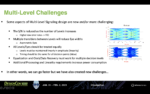
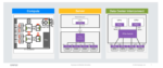
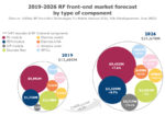
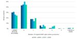
RF and microwave design is no longer confined to a few defense and aerospace EEs huddled in dark cubicles working with spreadsheets and primitive circuit simulators. Now, areas like 5G and automotive demand complex RF systems. Advanced RF and microwave EDA tools are taking on electromagnetic (EM), thermal, and power simulation,… Read More
Having known many of the top EDA CEOs during my semiconductor tenure the common traits I have found are brilliance, humility, endurance, and a sharp sense of humor. EDA solves so many problems, complex problem after complex problem, that it takes teams of incredibly smart people to solve them. Even more difficult is leading these… Read More
Way back in 2002 there was a study from Collett International Research on functional verification, and since 2010 the Wilson Research Group has continued that same kind of study with a new report every two years. What attracts me to this report is that it doesn’t just look at the installed base of one EDA vendor, instead it looks… Read More


Musk’s Orbital Compute Vision: TERAFAB and the End of the Terrestrial Data Center