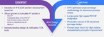
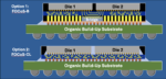
This year’s live semiconductor ecosystem conferences have been well attend and I expect the same for #61DAC next week. I will be at the conference from Sunday afternoon to Wednesday evening, if you would like to meet let me know. Networking is an important part of the semiconductor ecosystem so let’s make it happen.… Read More
Synopsys-AMD Webinar: Advancing 3DIC Design Through Next-Generation Solutions
Introduction of 2.5D and 3D multi-die based products are helping extend the boundaries of Moore’s Law, overcoming limitations in speed and capacity for high-end computational tasks. In spite of its critical function within the 3DIC paradigm, the interposer die’s role and related challenges are often neither fully comprehended… Read More
TSMC Advanced Packaging Overcomes the Complexities of Multi-Die Design
The TSMC Technology Symposium provides a worldwide stage for TSMC to showcase its advanced technology impact and the extensive ecosystem that is part of the company’s vast reach. These events occur around the world and the schedule is winding down. TSMC covers many topics at its Technology Symposium, including industry-leading… Read More
3DIC Verification Methodologies for Advanced Semiconductor ICs
At the recent User2user conference, Amit Kumar, Principal Hardware Engineer, Microsoft, shared the company’s experience from building a 3DIC SoC and highlighted Siemens EDA tools that were used. The following is a synthesis of core aspects of that talk.
3DIC Challenges
Despite the numerous advantages of 3DIC technology, its… Read More
Mastering Copper TSV Fill Part 3 of 3
Establishing void-free fill of high aspect ratio TSVs, capped by a thin and uniform bulk layer optimized for removal by CMP, means fully optimizing each of a series of critical phases. As we will see in this 3-part series, the conditions governing outcomes for each phase vary greatly, and the complexity of interacting factors means… Read More
Mastering Copper TSV Fill Part 2 of 3
Establishing void-free fill of high aspect ratio TSVs, capped by a thin and uniform bulk layer optimized for removal by CMP, means fully optimizing each of a series of critical phases. As we will see in this 3-part series, the conditions governing outcomes for each phase vary greatly, and the complexity of interacting factors means… Read More
AI System Connectivity for UCIe and Chiplet Interfaces Demand Escalating Bandwidth Needs
Artificial Intelligence (AI) continues to revolutionize industries, from healthcare and finance to automotive and manufacturing. AI applications, such as machine learning, deep learning, and neural networks, rely on vast amounts of data for training, inference, and decision-making processes. As AI algorithms become … Read More
Mastering Copper TSV Fill Part 1 of 3
Establishing void-free fill of high aspect ratio TSVs, capped by a thin and uniform bulk layer optimized for removal by CMP, means fully optimizing each of a series of critical phases. As we will see in this 3-part series, the conditions governing outcomes for each phase vary greatly, and the complexity of interacting factors means… Read More
Synopsys Accelerates Innovation on TSMC Advanced Processes
We all know that making advanced semiconductors is a team sport. TSMC can innovate the best processes, but without the right design flows, communication schemes and verified IP it becomes difficult to access those processes. Synopsys recently announced some details on this topic. It covers a lot of ground. The graphic at the top… Read More
Podcast EP223: The Impact Advanced Packaging Will Have on the Worldwide Semiconductor Industry with Bob Patti
Dan is joined by Bob Patti, the owner and President of NHanced Semiconductors. Previously, Bob founded ASIC Designs Inc., an R&D company specializing in high-performance systems and ASICs. During his 12 years with ASIC Designs he participated in more than 100 tapeouts. Tezzaron Semiconductor grew from that company, with… Read More
Rapidus, IBM, and the Billion-Dollar Silicon Sovereignty Bet