You are currently viewing SemiWiki as a guest which gives you limited access to the site. To view blog comments and experience other SemiWiki features you must be a registered member. Registration is fast, simple, and absolutely free so please,
join our community today!
WP_Term Object
(
    [term_id] => 23705
    [name] => 3D IC
    [slug] => 3dic
    [term_group] => 0
    [term_taxonomy_id] => 23705
    [taxonomy] => category
    [description] =>
    [parent] => 0
    [count] => 120
    [filter] => raw
    [cat_ID] => 23705
    [category_count] => 120
    [category_description] =>
    [cat_name] => 3D IC
    [category_nicename] => 3dic
    [category_parent] => 0
    [is_post] =>
)
At the 2024 TSMC OIP Ecosystem Forum, one of the technical talks by TSMC focused on maximizing 3DIC design productivity and rightfully so. With rapid advancements in semiconductor technology, 3DICs have become the next frontier in improving chip performance, energy efficiency, and density. TSMC’s focus on streamlining the… Read More
Synopsys made significant announcements during the recent TSMC OIP Ecosystem Forum, showcasing a range of cutting-edge solutions designed to address the growing complexities in semiconductor design. With a strong emphasis on enabling next-generation chip architectures, Synopsys introduced both new technologies and … Read More
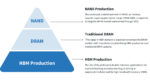
TechInsights has a new memory report that is worth a look. It is free if you are a registered member which I am. HBM is of great interest and there is a section on emerging and embedded memories for chip designers. Even though I am more of a logic person, memory is an important part of the semiconductor industry. In fact, logic and memory
…
Read More
Artificial intelligence (AI) and machine learning (ML) are evolving at an extraordinary pace, powering advancements across industries. As models grow larger and more sophisticated, they require vast amounts of data to be processed in real-time. This demand puts pressure on the underlying hardware infrastructure, particularly… Read More
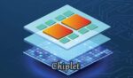
It is a well-known fact that chiplets provide several advantages over traditional monolithic chips. Despite these benefits, the transition to a chiplet-based design paradigm presents challenges that need coordinated efforts across the industry. In essence, collaborative efforts among various players involved are not … Read More
As the demand for higher performance computing solutions grows, so does the need for faster, more efficient data communication between components in complex multi-die system-on-chip (SoC) designs. In response to these needs, Synopsys has introduced the world’s fastest UCIe-based IP solution, capable of operating at a groundbreaking… Read More
The Universal Chiplet Interconnect Express™ (UCIe™) 1.0 specification was announced in early 2022 and a UCIe 1.1 update was released on August 8, 2023. This open standard facilitates the heterogeneous integration of die-to-die link interconnects within the same package. This is a fancy way of saying the standard opens the door… Read More
Despite NoCs being finely tuned in legacy subsystems, when subsystems are connected in larger designs or even across multi-die structures, differing traffic policies and system-level delays between NoCs can introduce new opportunities for deadlocks, livelocks and other hazards. Paul Cunningham (GM, Verification at Cadence),… Read More
In the rapidly evolving fields of high-performance computing (HPC) and artificial intelligence (AI), reducing time to market is crucial for maintaining competitive advantage. HBM3E systems play a pivotal role in this regard, particularly for hyperscaler and data center infrastructure customers. Alphawave Semi’s… Read More
Why Glass Substrates?by Sharada Yeluri on 08-13-2024 at 6:00 amCategories: 3D IC
The demand for high-performance and sustainable computing and networking silicon for AI has undoubtedly increased R&D dollars and the pace of innovation in semiconductor technology. With Moore’s Law slowing down at the chip level, there is a desire to pack as many chiplets as possible inside ASIC packages and get … Read More


Chemical Origins of Environmental Modifications to MOR Lithographic Chemistry