

Every generation of semiconductor innovation has relied on one fundamental principle: before a technology can be manufactured at scale, it must first be understood. That understanding comes through characterization.
For decades, characterization enabled process learning. It helped engineers understand transistor behavior,… Read More


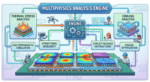

Enhancing Multi-Domain System Simulation with FMI Co-Simulation