
The semiconductor industry is entering a new era in which advanced packaging and chiplets-based architectures are becoming the primary drivers of system-level innovation. As traditional process-node scaling becomes increasingly complex and expensive, manufacturers are turning to heterogeneous integration, combining… Read More

Author: Kalar Rajendiran
Feed Forward Intelligence: Enabling Testability in the Chiplets Era

Agentic AI and the Future of Chip Design: From Productivity Tool to Engineering Partner

Highlights from a recent panel session moderated by Ed Sperling (Semiconductor Engineering) featuring Walden Rhines (Silvaco), Vincent Wong (Verific), Dave Kelf (Breker Verification Systems), Shelly Henry (MooresLab AI), Ann Wu (Silimate), and Cindy Cui (ChipAgents). The panel session was hosted by Electronic System … Read More
Customized Foundation IP Enables the Next Generation of Automotive Compute

As vehicles become increasingly software-defined, automotive semiconductor suppliers face growing pressure to deliver higher compute performance while maintaining strict requirements for power efficiency, reliability, and long-term product support. Advanced driver assistance systems (ADAS), electrification, … Read More
Engineering the Next Era of Semiconductor Innovation

The semiconductor industry is entering a transformative new phase, driven by the convergence of artificial intelligence, cloud computing, and increasingly complex chip architectures. That message took center stage during the keynote talks at the Siemens EDA User2User 2026 North America conference. Executives from Siemens,… Read More
SiFive’s P570 Gen 3 Pushes RISC-V Further Into the AI Era

With the launch of its new P570 Gen 3 processor family, SiFive is making a broader statement about the future of edge computing and the growing role of RISC-V in mainstream application processors. Rather than simply unveiling another CPU core, the company is positioning the P570 as a balanced-performance processor built specifically… Read More
From Point Solutions to Agentic AI Ecosystems: Semiconductor Process Control Depends on Its Past

Agentic AI is often presented as a revolutionary shift in semiconductor manufacturing, driven by large language models and generative AI. However, this framing overlooks an important reality: today’s advances are built on decades of prior work. As Jonathan Holt of PDF Solutions emphasizes in his recent keynote at the APCM 2026… Read More
RISC-V: From Niche Architecture to Strategic Foundation
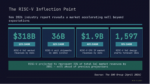
At the recent RISC-V Now by Andes conference, Aion Silicon’s presentation made one thing clear: RISC-V is no longer an emerging alternative but rather rapidly becoming foundational to modern silicon design. This conviction is not theoretical says Oliver Jones, CEO of Aion Silicon, who gave the talk. It is grounded in Aion Silicon’s… Read More
Synopsys and TSMC Deepen AI Design Alliance: What It Means

A recent announcement from Synopsys signals a meaningful escalation in the race to build next-generation AI hardware. The expanded collaboration between Synopsys and TSMC brings together silicon-proven IP, AI-driven design tools, and cutting-edge manufacturing processes in a tightly integrated effort to accelerate high-performance… Read More
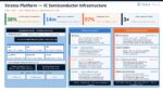
Connecting the Dots: Why RISC-V System Design Is Entering a New Era

At the recent RISC-V Now event hosted by Andes, the discussion underscored the fact that RISC-V is no longer just about instruction set architecture advantages or customizable cores. The real focus has moved up the stack to system-level design. This is where connectivity, integration, and security define whether an innovation… Read More
Rethinking ECAD IT Infrastructure: From Fragmentation to an Engineering Platform
The semiconductor industry is entering a new phase of complexity. Advanced nodes, heterogeneous integration, and AI-driven design workflows are placing unprecedented demands on engineering teams. While much of the focus remains on tools and methodologies, an equally critical constraint is emerging beneath the surface:… Read More


Why Huawei Says It Will Match TSMC’s Most Advanced Chips by 2031