You are currently viewing SemiWiki as a guest which gives you limited access to the site. To view blog comments and experience other SemiWiki features you must be a registered member. Registration is fast, simple, and absolutely free so please,
join our community today!
Teach Yourself Silvacoby admin on 05-12-2014 at 10:53 amCategories: EDA
In the dim and distant past, if you wanted to learn how to use a particular EDA tool then you would go on a training course. This would often be multiple days and often a significant dollar investment too. For most EDA companies, that option still exists and the big 3 have quite extensive training catalogs.
But nowadays it is often easier… Read More
Mounir Hahad Rejoins Silvacoby admin on 02-20-2014 at 4:16 pmCategories: EDA
Mounir Hahad just joined Silvaco as VP engineering. And when I say joined I really mean rejoined. I had a call with him to find out how that happened.
Mounir studied in France for a PhD in computer science on numerical computing. In 1995 the then-director of TCAD at Silvaco called him up having read some of his published papers. Silvaco… Read More
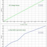
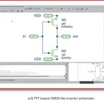
Simulation of Novel TFT Devicesby admin on 01-27-2014 at 5:45 pmCategories: EDA
Traditionally logic devices built on top of thin-film-transistors (TFTs) have used one type of device, either an NMOS a-Si: TFT (hydrogenated amorphous silicon) or a PMOS organic device. Recently a-Si:H and pentacene PMOS TFTs have been integrated into complementary logic structures similar to CMOS. This, in turn, creates… Read More
TowerJazz and Silvaco BFFby admin on 11-15-2013 at 1:04 pmCategories: EDA
Last week was the TowerJazz Technology Fair 2013. TowerJazz is the fourth biggest foundry in the world after TSMC, GF and UMC. They have fabs in Newport Beach (the old Jazz, itself with roots in Rockwell), two in Israel (the old Tower, with roots in National Semiconductor) and one in Japan (acquired from Micron). The technology fair… Read More
The Biggest Private EDA Companyby admin on 10-21-2013 at 5:02 pmCategories: EDA
I talked this morning with fellow Brit David Halliday. More importantly, he is CEO of Silvaco, which he thinks must be the biggest private EDA company in the world. He didn’t reveal their revenue numbers but they have around 250-300 people and are profitable so you can make your own estimate.
David became CEO when Ivan Pesic,… Read More
Sagantec is the leading EDA provider of process migration solutions for custom IC design. Sagantec’s EDA solutions enable IC designers to leverage their investment in existing physical design IP and accomplish dramatic time and effort savings in the implementation of custom, analog, mixed-signal and memory circuits… Read More
The earthquake and subsequent tsunami that devastated Japan on March 11[SUP]th[/SUP], 2011 will have far reaching ramifications around the world for years to come. People have asked me how this disaster will affect the semiconductor industry so I will try and summarize it in this blog.
First the foundries:
According to TSMC: … Read More
San Jose, Calif., [DATE], 2011 – SemiWiki.com today announced that Mentor Graphics, a world leader in electronic hardware and software design solutions, will participate in the SemiWiki.com global social media platform aimed at facilitating mass communication for electronic design professionals through Web 2.0 technologies.… Read More


Tesla and Samsung Relationship Update