The CHIPS and Science Act has allocated $11 billion for semiconductor R&D, including for advanced packaging and AI-driven design. Companies should apply now.
In 2022, the United States signed the $50 billion Chips and Science Act. Under the act, the National Institute of Standards and Technology (NIST), which is part of the US Department of Commerce, is administering $11 billion for research and development projects. Befitting its name, the Chips R&D effort seeks to foster innovation (research) and commercialization (development). A third goal is to nurture the workforce. Chips R&D targets five areas:
- The National Semiconductor Technology Center (NSTC), a public-private consortium to provide R&D facilities and equipment.
- The National Advanced Packaging Manufacturing Program (NAPMP).
- The Chips Manufacturing USA Institute to develop digital twin technologies for semiconductor manufacturing.
- Chips Metrology, which applies the science of measurement (a key part of NIST) to semiconductor materials, packaging, and production.
Funding Opportunities and Deadlines
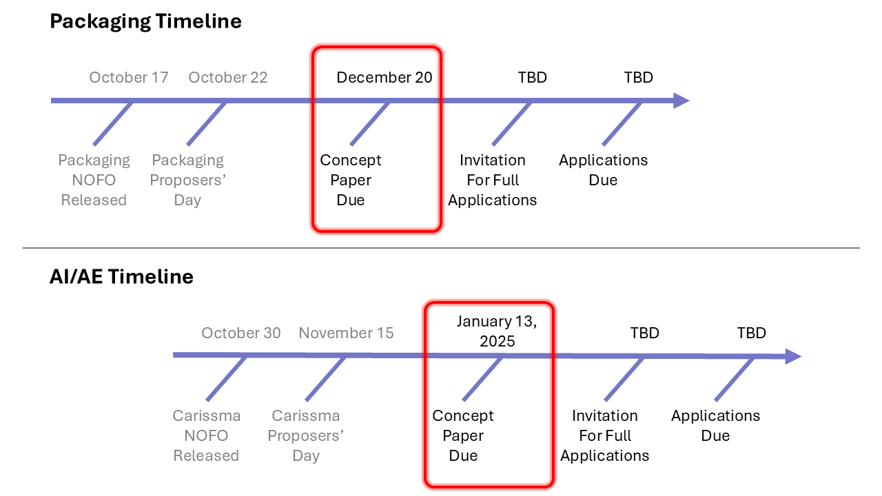
NIST is doling out R&D awards in a notice of funding opportunity (NOFO) series. NOFOs from earlier this year target package substrates and establishment of the Chips Manufacturing USA Institute. Two open NOFOs include one applying artificial intelligence (AI) and autonomous experimentation (AE) to manufacturing and another targeting advanced packaging. In both cases, applicants’ first step is to submit a concept paper. Due dates are January 13, 2025, and December 20, 2024, for the AI/AE and packaging NOFOs, respectively, as Figure 1 shows. Local to NIST and having a writing background, I’m available to work with applicants on their submissions.

The Chips AI/AE for Rapid, Industry-Informed Sustainable Semiconductor Materials and Processes (Carissma) competition expects to disburse $100 million to organizations developing semiconductor materials. They must outperform existing materials and be better for the environment. The timeline is short—only five years for an investment to produce something the industry can test. Carissma requires the projects to be university led and apply AI/AE techniques.
Pushing Packaging Boundaries
Part of the NAPMP, the packaging NOFO will provide multiple awards totaling $1.55 billion and spans five R&D areas (RDAs in government lingo):
- Equipment, tools, processes, and process integration
- Power delivery and thermal management
- Connector technology, including photonics and radio frequency (RF)
- Chiplets ecosystem
- Codesign/electronic design automation (EDA)
Area Four indicates the NOFO’s thrust: extending the multi-die (and multidimensional) packaging technology found in products such as the AMD MI300X, Intel Ponte Vecchio, and Nvidia Blackwell. Examining this area also reveals the program’s vision and assumptions: thousands of wires will connect chiplets, packages will be ultra-large and house a thousand chiplets, and chiplets will be functionally and physically heterogeneous. It’s an unusual vision considering systems today contain tens or possibly hundreds of chips per chassis—not thousands of chips. For a few more details on the chiplet RDA, see my post at https://xpu.pub/2024/10/24/chips-act-packaging/.
The other four areas proceed from this vision. The first has two categories that applicants can address: either a specific step in the packaging flow or an end-to-end process linking the individual steps. The second offers four objectives that applicants can address, including actual power-delivery and thermal-management solutions and models.
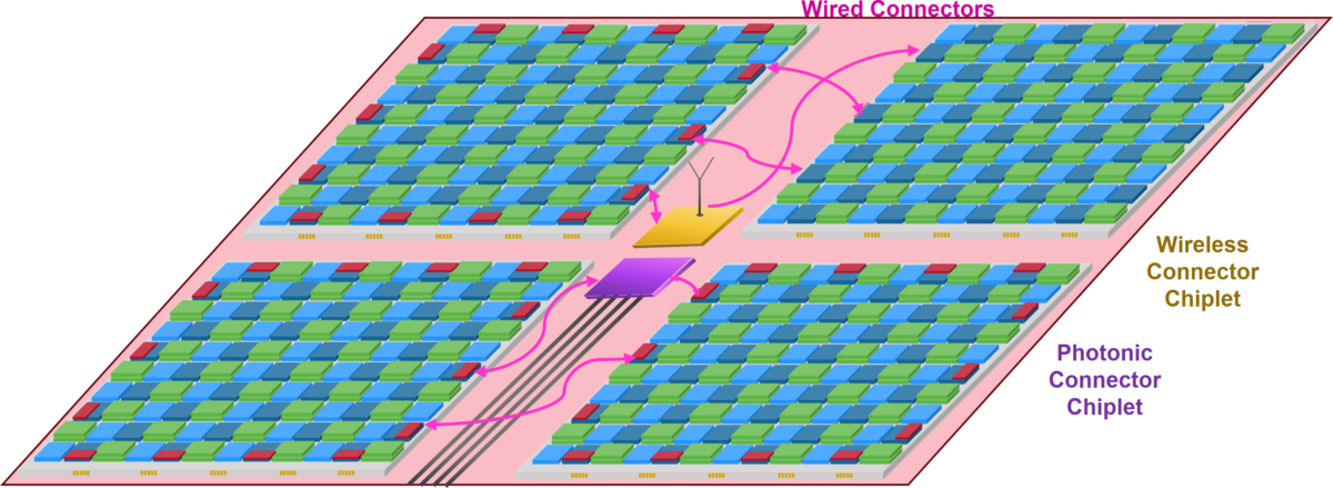
Area Three addresses interpackage (not intrapackage) interconnect and covers three scales: less than 25 mm, less than 1 m, and less than 1 km. For the shortest distance, the goal is 100 Gb/s per channel and a shoreline bandwidth density of 10 Tb/s per mm. The latter parameter is the challenging one; 224 Gbps serdes are already in production. For the sub-meter and sub-kilometer scales, the minimum bandwidth is 100 Tb/s. A further challenge for all three distances is to achieve a 0.1 picojoule per bit ceiling. As Figure 2 shows, the interconnect among packages can be wired, wireless (RF), or photonic.

The final area is for software tools to aid design, security, resilience (e.g., fault tolerance), and integration, verification, and validation (IV&V). The EDA tools must handle designs employing any substrate, a thousand chiplets, 24-high chiplet stacks, a mixture of functionality (digital, analog, and optical), and various other components.
Write 10 Pages, Get $150 Million
It’s unusual for the United States to implement an industrial policy as directly interventionist as the Chips Act. Left alone, companies undoubtedly would develop technologies, but the Chips R&D effort is an opportunity for them to accelerate programs. Although applicants must be US-based and the act aims to bolster US manufacturing, operations and people can also be elsewhere. Recognizing this, attendees at the recent NAPMP NOFO conference came not only from American organizations but also from European and Asian companies with an affiliated US entity.
As noted above, the next step for those interested in the Carissma and NPAMP packaging NOFOs is to submit a concept paper. It must be no longer than 10 pages, making it possible to crank out in less than a month. It must broadly discuss the applicant’s project, including the technical area, execution plan, and budget. The Chips R&D review board will consider submissions on the basis of economic and national security, technical merit, project management, and ultimate impact. Concepts deemed meritorious then must submit a full application for final review. Grants will range up to $150 million, a significant sum for a large company and transformational for a smaller one. I urge US entities to apply. As noted above, I’m available to assist with concept papers and have the advantage of being local to NIST.
Joseph Byrne is an independent analyst and consultant. For more information, see xampata.com.
Also Read:
Synopsys-Ansys 2.5D/3D Multi-Die Design Update: Learning from the Early Adopters
Sarcina Democratizes 2.5D Package Design with Bump Pitch Transformers
Analog Bits Builds a Road to the Future at TSMC OIP
Navigating Resistance Extraction for the Unconventional Shapes of Modern IC Designs
Share this post via:


Musk’s Orbital Compute Vision: TERAFAB and the End of the Terrestrial Data Center