The semiconductor industry is experiencing rapid evolution, driven by the proliferation of IoT applications, image sensors, photonics, MEMS applications, 3DIC and other emerging technologies. This growth has dramatically increased the complexity of integrated circuit (IC) design. One aspect of this complexity is the use of unconventional, non-Manhattan layout structures to achieve optimal functionality and performance.
Non-Manhattan routing examples
3DICs—As technology advances and the limits of Moore’s Law approach, 3DICs allow designers to decompose architecture into smaller chiplets. These are integrated into a single package, offering higher integration density, faster interconnect speeds, lower power consumption, higher bandwidth data movement, better thermal management, and overall reduced costs. A key feature of 3DIC design is the use of curvilinear shapes for non-Manhattan routing in interconnects and redistribution layers (RDL) among through-silicon vias (TSVs) and micro-bumps, which enhances flexibility and performance but poses new challenges for design tasks like resistance extraction.
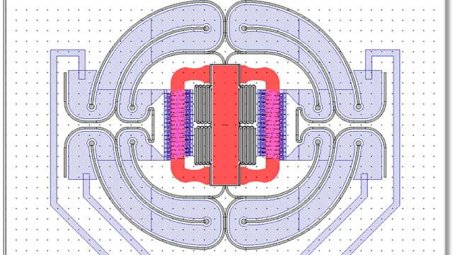
Image sensors and MEMS designs—Image sensors, utilized in devices like digital cameras, smartphones, and surveillance systems, demand high image recognition capabilities. Designers incorporate wide polygons in layout designs to achieve this. These wide photodiode polygons gather more light, resulting in high-resolution, low-noise images with high dynamic range and low power consumption. MEMS designs utilize curvilinear shapes and unconventional geometries for a broad range of applications in mechanical, optical, magnetic, fluidic, and biomedical fields. An example of a MEMS layout is shown in figure 1.

However, the use of wide polygons in image sensors and complex structures in MEMS introduce significant challenges for resistance extraction, which is an important part of ensuring the design’s reliability. Traditional field solvers, though effective, often require long run times and are unsuitable for full-chip verification due to computational complexity. Designers need to leverage the newer fracturing techniques have emerged to improve accuracy and efficiency in resistance extraction for different applications.
Resistance extraction for design reliability
Resistance extraction is crucial for IC design physical verification. Accurate resistance modeling is essential for predicting circuit behavior through simulation, ensuring the overall reliability and accuracy of circuit performance. As interconnect sizes decrease, the impact of parasitic resistance becomes more pronounced.
Accurate resistance extraction ensures the reliability, performance, and functionality of ICs across various downstream flows, including timing analysis, power analysis, electromigration, signal integrity analysis, thermal analysis, and noise analysis. Timing analysis, for instance, relies on accurate parasitic resistance extraction to estimate signal delays, identify critical paths, and ensure proper timing closure.
Parasitic resistance extraction faces significant challenges, such as increasing design complexity, aggressive shrinking in feature sizes, and the presence of non-standard geometries requiring special handling through advanced fracturing techniques.
Evolving fracturing techniques for accurate resistance extraction
For precise resistance extraction, it is essential to divide geometries into smaller fragments, allowing detailed analysis and accurate estimation of parasitic resistances. This process, known as fracturing, breaks down complex geometries into smaller parts. The extraction process captures the complexities and details of individual components and interconnects, leading to a more precise determination of parasitic resistances. These techniques include 1D fracturing, 2D fracturing, and more advanced methods designed to handle curvilinear shapes.
- 1D fracturing:
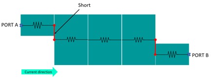
1D fracturing involves dividing a route into multiple fractures in one dimension based on current direction. Resistance is calculated for each fracture based on its length, width, and the sheet resistance of the layer. While efficient for standard geometries, 1D fracturing may introduce inaccuracies for shapes with non-uniform current flow or irregular cross-section profiles (figure 2)

Electronic design automation vendors strive to handle non-uniform current distribution in 1D fracturing by using complex models and algorithms, improving resistance accuracy even in cases of non-uniform current distribution.
- 2D fracturing:
2D fracturing handles planar structures and slotted metals by fracturing shapes into smaller polygons that cover the planar regions. This enables accurate parasitic resistance extraction for planar and slotted structures.
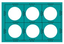
Considering slotted conductors, 2D fracturing creates a mesh of resistors around the slots, offering more accurate resistance extraction than simple 1D fracturing (figure 3).

- Advanced fracturing:
Curvilinear shapes are critical in applications such as analog and RF designs, antenna designs, MEMS devices, 3DIC and optical waveguides. Advanced fracturing techniques handle the complexity of these structures more effectively than traditional methods.
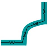
Advanced fracturing methods, such as fracturing in the direction of the polygon, break structures into smaller elements aligning with polygon boundaries, allowing more accurate resistance extraction. Figure 4 illustrates fracturing polygon for a curved conductor.

Best practices for next-generation extraction tools
To ensure accurate resistance extraction, consider design automation tools that integrate newer fracturing techniques that accommodate non-Manhattan routes.
A rule-based extraction engine applies heuristics to determine the current direction and subsequently applies 1D fracturing, then generates nodes across the current direction and calculates resistance between them, resulting in precise P2P resistance values for uniform structures, which are common in most designs.
To effectively handle unconventional structures, parasitic extraction tools should allow users specify the application of 2D fracturing for a conductor layer under a specified marker layer. This approach involves applying a 2D mesh to the conductor layer to enable accurate P2P results for unconventional structures.
Additionally, an advanced flow should be introduced to handle curvilinear shapes and complex structures, eliminating the need for a field solver and maintaining reasonable runtimes. This approach ensures accurate resistance extraction for various design scenarios, providing reliable performance and efficiency in IC designs.
Summary
Accurate measurement of interconnect resistance is fundamental for ensuring circuit performance and reliability. Designers need advanced tools to handle curvilinear shapes and complex structures, enabling quick and accurate point-to-point resistance extraction for the full layout.
For more information download the full technical paper HERE.
Also Read:
SystemVerilog Functional Coverage for Real Datatypes
Automating Reset Domain Crossing (RDC) Verification with Advanced Data Analytics
Smarter, Faster LVS using Calibre nmLVS Recon
Share this post via:


