

Also Known As: TSMC 1.6 nm, Angstrom-class node
Node Class: Leading-edge logic (1.6 nm)
Transistor Type: Nanosheet GAAFET (Gate-All-Around Field-Effect Transistor)
Backside Power Variant: Integrates Super Power Rail (SPR) backside power delivery
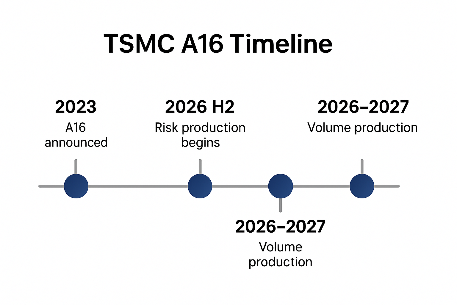
Launch Schedule: Risk production in 2026, volume production in H2 2026–2027
Predecessor: TSMC N2P/A14 (2 nm-class)
Successor Candidate: Later 1.4 nm A14, CFET nodes
Overview
TSMC’s A16 is the first Angstrom-class chipmaking node, representing a major leap in semiconductor manufacturing. It succeeds the N2 family by integrating both second-gen GAAFET transistors and SPR backside power distribution, delivering enhanced performance, power efficiency, and density suited for AI, HPC, and premium consumer designs
Features & Architecture
-
Super Power Rail (SPR): A backside power network that decouples signal routing from power delivery, enabling tighter routing and improved IR drop
-
GAAFET Nanosheet Transistors: Refined from N2, providing improved gate control and drive current with vertical stacking
-
Lithography: Based on current EUV equipment, no High‑NA EUV required
-
NanoFlex Compatibility: Fully supports flexible cell layouts and optimized PPA, like N2P
Performance, Power & Density (PPA)
Compared to N2P, A16 offers:
-
8–10% higher performance at equal voltage/complexity
-
15–20% lower power consumption at the same performance
-
7–10% increased density (approx. 1.07×–1.10×)
Timeline
| Year | Milestone |
|---|---|
| 2023 | A16 officially announced |
| 2026 H2 | Risk production begins; SPR introduced (replaces SPR-deferral in N2P) |
| 2026–2027 | Volume production begins for AI/HPC/5.5″ interposer designs |
| 2028–2030 | A16 production extends to U.S. fabs (Fab 21, Arizona) |
Ecosystem & Adoption
-
EDA/IP Support: Certified by Synopsys and Cadence for analog, digital, 3D-IC/chiplet design flows
-
Initial Design Wins: Attracting Apple, OpenAI, AMD, Nvidia for AI/dense compute products
-
Fab 21 (Arizona) includes A16/N2/N2P-capable tooling, aiming for domestic production from ~2028
Strategic Importance
-
Angstrom-Class Leadership: Introduces backside power early, surpassing N2P’s deferred SPR
-
No High‑NA EuV Dependency: Delivers full-node PPA gains using established EUV platforms
-
AI/HPC Positioning: SPR + GAAFET combination ideal for compute-heavy dies with deep routing and high power density.
Comparison: N2P vs. A16
| Metric | N2P | A16 (vs. N2P) |
|---|---|---|
| Transistors | GAAFET + NanoFlex | Same GAAFET with SPR |
| Power Delivery | Front/backside deferred | SPR backside integrated |
| Performance | Baseline 2 nm-class | +8–10% |
| Power Efficiency | Baseline | –15–20% |
| Density Increase | Baseline | +7–10% |
Future Outlook
-
A16P may bring further power-delivery advances (e.g., tighter SPR).
-
TSMC planning A14 (1.4 nm) similar but denser node
-
Long-term roadmap includes Forksheet FET, CFET, and 3+D-IC integration beyond A16.
Summary
TSMC A16 is TSMC’s pioneering Angstrom-scale node integrating GAAFET nanosheets with Super Power Rail backside power, delivering substantial PPA gains without relying on High‑NA EUV. Slated for H2 2026 volume production, A16 positions TSMC at the forefront of advanced foundry technology for AI, HPC, and advanced packaging.
Share this post via:


Musk’s Orbital Compute Vision: TERAFAB and the End of the Terrestrial Data Center