
Overview
TSMC N5 (5-nanometer process node) is a high-volume FinFET-based semiconductor manufacturing technology developed by Taiwan Semiconductor Manufacturing Company (TSMC). It succeeded the N7 (7nm) family and introduced substantial improvements in performance, power, and transistor density.
N5 is widely regarded as the most successful advanced node of its generation, powering numerous flagship SoCs from Apple, AMD, Qualcomm, and others since 2020. It laid the foundation for future derivatives such as N4, N3, and N2.
Key Milestones
| Year | Event |
|---|---|
| 2018 | Risk production for N5 begins |
| 2020 (Q2) | Volume production starts (Apple A14 chip) |
| 2020–2022 | Mainstream adoption across consumer, HPC, and automotive chips |
| 2021–2024 | Extended with N5P, N4, N4P, N4X variants |
Technical Specifications
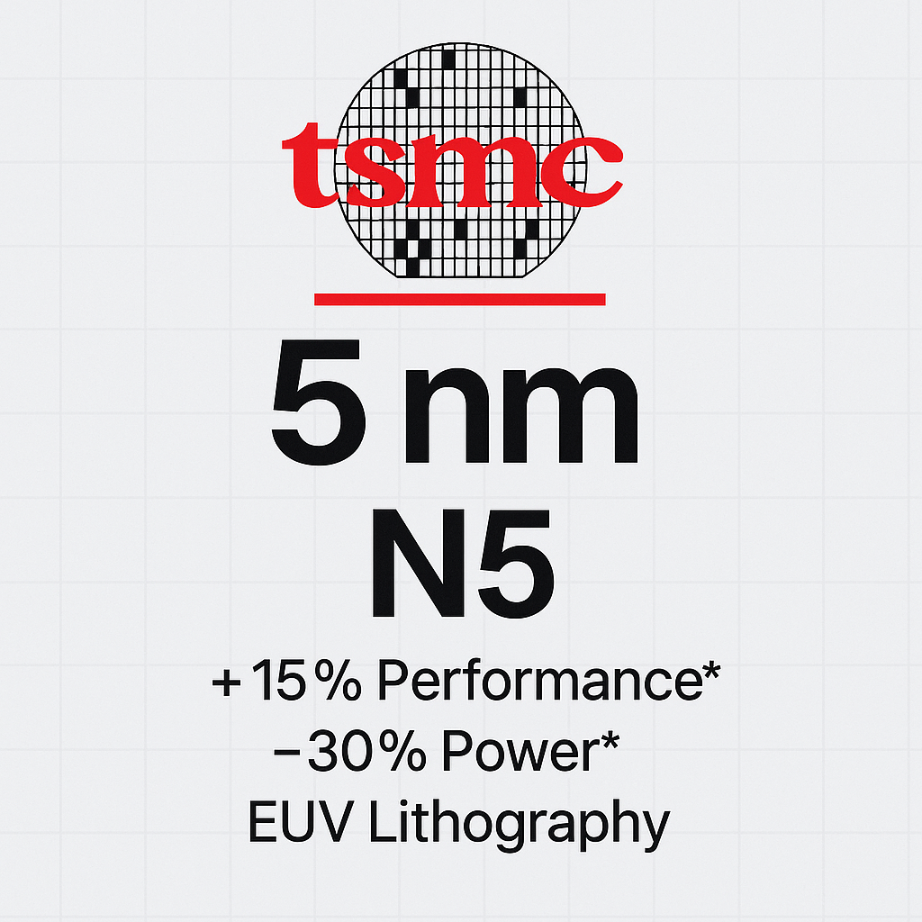
| Feature | TSMC N5 | Improvement Over N7 |
|---|---|---|
| Transistor Type | FinFET | — |
| Density | ~171 million transistors/mm² | ~80% increase |
| Performance Gain | ~15% faster | Same power |
| Power Reduction | ~30% lower | Same speed |
| Lithography | EUV (Extreme Ultraviolet Lithography) | More layers (10–14 EUV layers) |
| Metal Pitch Shrink | Yes | Tighter BEOL scaling |
| Contacted Gate Pitch | ~51nm | ~Down from 57nm on N7 |
TSMC’s N5 was one of the first nodes to use EUV extensively, improving pattern fidelity and reducing mask count.
Derivatives of N5
| Node | Description | Introduced |
|---|---|---|
| N5P | Performance-enhanced N5; ~5% speed boost or 10% lower power | 2021 |
| N4 | Optical shrink of N5; compatible design rules, better density | 2022 |
| N4P | Enhanced N4 with ~11% performance over N5 | 2022 |
| N4X | High-performance N4 for HPC (e.g., >1V operation) | 2023 |
All derivatives maintain FinFET architecture, targeting different markets (mobile, HPC, automotive).
Lithography Details
-
EUV usage: Significantly more than N7+ (7nm with limited EUV).
-
Patterning simplification: Replaced complex multi-patterning DUV steps.
-
Yield benefit: Fewer process steps → reduced defect rates.
-
Back-end-of-line (BEOL): Improved metal stack with lower RC delay.
Power-Performance-Area (PPA)
| Metric | Value |
|---|---|
| Density | ~1.8x over N7 |
| Performance | +15% over N7 |
| Power Efficiency | -30% vs N7 |
Measured at iso-power and iso-frequency conditions
Adoption and Major Users
✅ Apple
-
A14 Bionic (2020) – first chip on N5
-
M1 series (M1, M1 Pro, M1 Max) – Macs and iPads
-
A15 Bionic (2021) – on N5P
-
M2 (2022) – N5P or N4 (conflicting reports)
✅ AMD
-
Chiplets for future SoCs expected to use N5 and N4.
✅ Qualcomm
-
Snapdragon 8 Gen 1+ (TSMC version) and newer high-end SoCs moved to N4/N5P.
✅ MediaTek
-
Dimensity 9000 series (5nm/N4), adopted N5 for premium mobile chipsets.
✅ Broadcom, Marvell, NVIDIA
-
Adopted N5/N4P for networking ASICs and AI accelerators.
Comparison with Other Nodes
| Feature | TSMC N7 | TSMC N5 | TSMC N4 | Samsung 5LPE |
|---|---|---|---|---|
| Transistor Type | FinFET | FinFET | FinFET | FinFET |
| EUV Usage | Limited | High (10–14 layers) | High | Limited |
| Density | ~90M/mm² | ~171M/mm² | ~185M/mm² | ~125M/mm² |
| Performance | Baseline | +15% vs N7 | +10% vs N5 | ~10% vs N7 |
| Power | — | ~30% lower than N7 | ~35% lower | ~20–25% lower |
TSMC’s N5 is generally superior to Samsung’s 5nm node, especially in logic density and EUV maturity.
Challenges
-
Mask cost: High due to more EUV layers and complex OPC.
-
Design transition: Required new design flows and IP libraries.
-
Yield ramp: Initially lower than N7 but quickly matured.
Tools & Ecosystem
-
Supported by all major EDA vendors:
-
Cadence, Synopsys, Siemens, Ansys
-
-
TSMC’s Open Innovation Platform (OIP) provided:
-
PDKs (Process Design Kits)
-
Reference flows
-
Silicon-validated IP
-
Role in TSMC’s Roadmap
| Node | Type | Year |
|---|---|---|
| N7 | FinFET | 2018 |
| N5 | FinFET + EUV | 2020 |
| N4 | N5 shrink | 2022 |
| N3 | Advanced FinFET | 2023 |
| N2 | GAA + BSPDN | 2025 |
N5 marked the transition point to EUV-centric manufacturing and set the stage for finer nodes like N3 and N2.
Applications Enabled
-
Smartphone SoCs (Apple, Qualcomm, MediaTek)
-
AI accelerators and NPUs
-
CPU and GPU chiplets
-
Networking ASICs (Broadcom, Marvell)
-
Automotive SoCs (ADAS processors)
Summary
TSMC N5 is a landmark node in semiconductor history due to its:
-
Widespread adoption across industries
-
Strong PPA benefits
-
Reliable EUV production at scale
-
Role in enabling Apple’s M1 chip revolution
It continues to be relevant in 2024–2025 due to its derivatives (N4/N4P/N4X) and its balance of performance, cost, and yield maturity.


Silicon Insurance: Why eFPGA is Cheaper Than a Respin — and Why It Matters in the Intel 18A Era