Overview
TSMC N3 is the 3-nanometer FinFET semiconductor manufacturing node developed by Taiwan Semiconductor Manufacturing Company (TSMC). It is a major milestone in TSMC’s process technology roadmap and represents the first step into the 3nm era, succeeding the N5 and N4 nodes.
Unlike Samsung, which introduced Gate-All-Around (GAA) technology with its 3nm, TSMC continues to use FinFET transistors at the N3 generation. GAA will debut in TSMC’s N2 (2nm) node, expected in late 2025.
Technical Highlights
| Feature | TSMC N3 (N3B Baseline) | Compared to N5 |
|---|---|---|
| Transistor Type | FinFET | — |
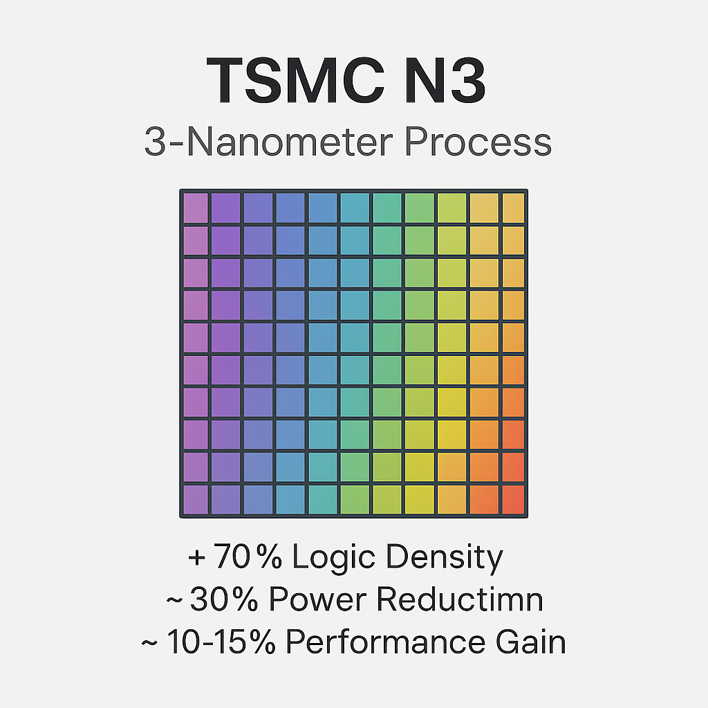
| Density Increase | +70% logic density | vs. N5 |
| Power Consumption | ~30% lower | at same speed |
| Performance | ~10–15% faster | at same power |
| EUV Layers | ~25–28 EUV layers | vs. ~14 in N5 |
| Gate Pitch Shrink | Tightened metal and poly pitch | Enables higher density |
| SRAM Cell Size | ~5–10% smaller | vs. N5 |
| BEOL Scaling | Advanced multi-patterned metallization | More RC delay optimized |
SRAM Comparison: TSMC N3 vs. N5
| Feature | TSMC N5 | TSMC N3 (N3B) | TSMC N3E |
|---|---|---|---|
| SRAM Bitcell Size | ~0.021 µm² | ~0.0199 µm² | ~0.021 µm² |
| Area Scaling | – | ~5–10% smaller vs. N5 | Roughly same as N5 |
| Performance | Mature, good Vmin behavior | Lower Vmin, but more variability | Improved stability vs. N3B |
| Leakage Power | Baseline | Slightly higher | Lower than N3B |
| Yield | High | Lower for SRAM than logic | Better than N3B, but not as strong as N5 |
Process Notes:
-
N3B is not IP-compatible with N5/N4, unlike N3E.
-
Contacted poly pitch (CPP) and metal pitch were both aggressively scaled.
-
Still uses DUV + EUV lithography, but with significantly more EUV steps than N5.
-
Introduces tighter layout design rules, requiring extensive PPA co-optimization.
N3 Platform Variants
TSMC has extended the N3 platform into multiple specialized versions:
| Variant | Description | Key Features |
|---|---|---|
| N3B | Baseline node, used by Apple first | Most EUV layers, higher density, lower yield |
| N3E | Enhanced version, mass-market ready | Lower cost, better yield, improved performance |
| N3P | Performance-focused N3E derivative | Targeted at HPC and AI SoCs |
| N3X | High-performance extension | For ultra-high-performance computing |
| N3AE | Automotive-grade N3E (planned) | For ADAS and vehicle processors |
Manufacturing & Supply Chain
-
Main Fab: Fab 18, Tainan, Taiwan
-
Risk Production Start: Q3 2021 (N3B)
-
Volume Production (N3B): Late 2022 (limited customers)
-
Volume Production (N3E): Late 2023 onward
-
Geographic Expansion:
-
N3 not expected to be deployed at Arizona Fab 21 (focused on N4/N5).
-
N3/N2 to remain in Taiwan due to fab complexity and talent concentration.
-
Real-World Adoption
🔹 Apple
-
A17 Pro (iPhone 15 Pro/Pro Max) — First mass-produced chip on N3B
-
M3 Series (M3, M3 Pro, M3 Max, M3 Ultra) — 2023–2024 Mac chips on N3B/N3E
-
M4 Series — 2024–2025 on N3E
🔹 Other Expected Customers
| Company | Notes |
|---|---|
| Intel | Planning to use N3E/N3P for chiplets in upcoming CPUs and SoCs |
| AMD | Expected to move GPU and CPU chiplets to N3P in 2025–2026 |
| MediaTek | Flagship Dimensity SoCs on N3E starting in 2024 |
| Qualcomm | Evaluating N3P/N3X; may stay on N4/N5 until mid-2025 |
| Broadcom, Marvell, NVIDIA | Targeting N3E and N3X for networking, AI accelerators, and HPC |
Challenges and Lessons from N3B
TSMC’s N3B was more aggressive in design and less optimized for yield, leading to:
-
High defect rates initially, making it viable only for large-volume, high-margin customers like Apple.
-
Reluctance from other chipmakers to adopt until N3E.
TSMC acknowledged this by pivoting future customers toward N3E, which:
-
Has better performance-per-watt
-
Lower manufacturing cost per wafer
-
Is design-rule compatible with future N3 derivatives (P, X, AE)
EDA & IP Ecosystem
-
Full PDK (Process Design Kit) support from:
-
Cadence (Innovus, Spectre)
-
Synopsys (Fusion Compiler, PrimeTime)
-
Ansys (RedHawk, Totem)
-
-
IP library vendors providing:
-
Standard cell libraries
-
SRAM compilers
-
Interface IP (DDR5, LPDDR5, PCIe 5.0/6.0, USB4, CXL)
-
TSMC also expanded its Open Innovation Platform (OIP) to support early tapeouts and test chips from partners on N3E.
Roadmap: N3 to N2 and Beyond
| Node | Year | Key Change |
|---|---|---|
| N3B | 2022 | First-generation 3nm, high EUV |
| N3E | 2023 | Enhanced node, better yield |
| N3P | 2024 | Performance-focused N3E |
| N3X | 2025 | High-performance for AI/HPC |
| N2 | Late 2025 (risk), 2026 (volume) | GAA (Nanosheet) + Backside Power Delivery |
-
N2 will be TSMC’s first nanosheet (gate-all-around) node.
-
Introduces backside power delivery network (BSPDN) for power integrity and IR drop reduction.
Comparison With Competitors
| Company | Node | Type | Notes |
|---|---|---|---|
| TSMC | N3B/N3E | FinFET | Most mature, Apple-exclusive early |
| Samsung | SF3E/SF3 | GAA | First to market with GAA, but lower yield/adoption |
| Intel | Intel 3 | FinFET | Matches TSMC N5/N3E in performance; used for internal and foundry clients |









Captain America: Can Elon Musk Save America’s Chip Manufacturing Industry?