You are currently viewing SemiWiki as a guest which gives you limited access to the site. To view blog comments and experience other SemiWiki features you must be a registered member. Registration is fast, simple, and absolutely free so please,
join our community today!
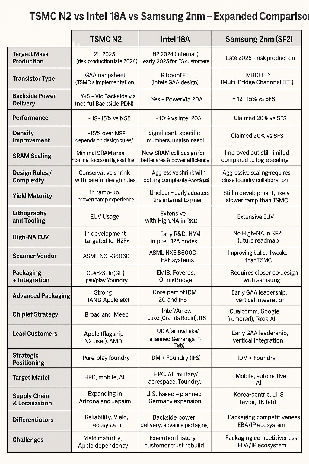
| Category |
TSMC N2 |
Intel 18A |
Samsung 2nm (SF2) |
| Target Mass Production |
2H 2025 (risk production late 2024) |
H2 2024 (internal); early 2025 for IFS customers |
Late 2025 – risk production |
| Transistor Type |
GAA nanosheet (TSMC’s implementation) |
RibbonFET (Intel’s GAA design) |
MBCFET™ (Multi-Bridge Channel FET) |
| Backside Power Delivery |
Yes — via Backside via (not full backside PDN) |
Yes — PowerVia, true backside power, full-scale |
Partially implemented, full backside may arrive in SF1.4 |
| Performance Uplift |
~10–15% vs N3E |
>10% vs Intel 20A |
~12–15% vs SF3 |
| Density Improvement |
~15% over N3E (depends on design rules) |
Significant; specific numbers undisclosed |
Claimed 20% vs SF3 |
| SRAM Scaling |
Minimal SRAM area scaling; focus on logic scaling |
New SRAM cell design for better area & power efficiency |
Improved but still limited compared to logic scaling |
| Design Rules / Complexity |
Conservative shrink with careful design rules |
Aggressive shrink with tooling complexity (PowerVia+GAA) |
Aggressive scaling, requires close foundry collaboration |
| Yield Maturity |
In ramp-up, proven ramp experience (N3E base) |
Unclear — early adopters are internal to Intel |
Still in development, likely slower ramp than TSMC |
🔬 Lithography and Tooling
| Category |
TSMC N2 |
Intel 18A |
Samsung SF2 |
| EUV Usage |
Extensive EUV, including 2nd-gen |
Extensive, with High-NA in R&D |
Extensive EUV |
| High-NA EUV |
In development (targeted for N2P) |
Early R&D; HVM in post-18A nodes |
No High-NA in SF2; future roadmap |
| Scanner Vendor |
ASML NXE:3600D |
ASML NXE:3600D + EXE systems |
ASML NXE:3600D |
🧱 Packaging + Integration
| Category |
TSMC N2 |
Intel 18A |
Samsung SF2 |
| Advanced Packaging |
CoWoS, InFO, SoIC, System-on-Wafer |
EMIB, Foveros, Omni-Bridge |
I-Cube, X-Cube |
| Chiplet Strategy |
Strong (AMD, Apple, etc.) |
Core part of IDM 2.0 and IFS |
Emerging; used for Exynos, others |
| Foundry Ecosystem |
Industry-leading |
Rapidly growing with IFS push |
Improving but still weaker than TSMC |
🧑💻 Design Ecosystem
| Category |
TSMC N2 |
Intel 18A |
Samsung SF2 |
| EDA & PDK Maturity |
Highly mature |
Catching up quickly |
Requires closer co-design with Samsung |
| IP Ecosystem |
Broad and deep |
Still growing |
Improving, but limited vs. TSMC |
| Lead Customers |
Apple (flagship N2 user), AMD |
Intel (Meteor Lake/Arrow Lake), IFS |
Qualcomm, Google (rumored), Tesla AI |
🏁 Strategic Positioning
| Category |
TSMC N2 |
Intel 18A |
Samsung SF2 |
| Business Model |
Pure-play foundry |
IDM + Foundry (IFS) |
IDM + Foundry |
| Target Markets |
HPC, mobile, AI |
HPC, AI, military/aerospace, foundry |
Mobile, automotive, AI |
| Supply Chain & Localization |
Expanding in Arizona and Japan |
U.S.-based + planned Germany expansion |
Korea-centric, U.S. (Taylor, TX fab) |
| Differentiators |
Reliability, yield, ecosystem |
Backside power delivery, advanced packaging |
Early GAA leadership, vertical integration |
| Challenges |
Yield maturity, Apple dependency |
Execution history, customer trust rebuild |
Packaging competitiveness, EDA/IP ecosystem |
🧠 Summary
-
TSMC N2 is the most conservative and customer-proven roadmap with strong Apple partnership and robust chiplet/packaging offerings. Focus is on reliability and yield.
-
Intel 18A is technically aggressive, combining RibbonFET + PowerVia, and targeting leadership in performance/watt. Foundry customer wins and IFS maturity are key.
-
Samsung SF2 brings early GAA experience and solid EUV toolchain but needs to scale its ecosystem and yields to challenge TSMC in premium mobile and AI workloads.
Share this post via:







Captain America: Can Elon Musk Save America’s Chip Manufacturing Industry?