

Also known as: TSMC 1.4nm, A14 process node
Node class: Advanced logic technology (1.4nm)
Foundry: Taiwan Semiconductor Manufacturing Company (TSMC)
Expected HVM (High Volume Manufacturing): 2028
Predecessor: TSMC N2 (2nm)
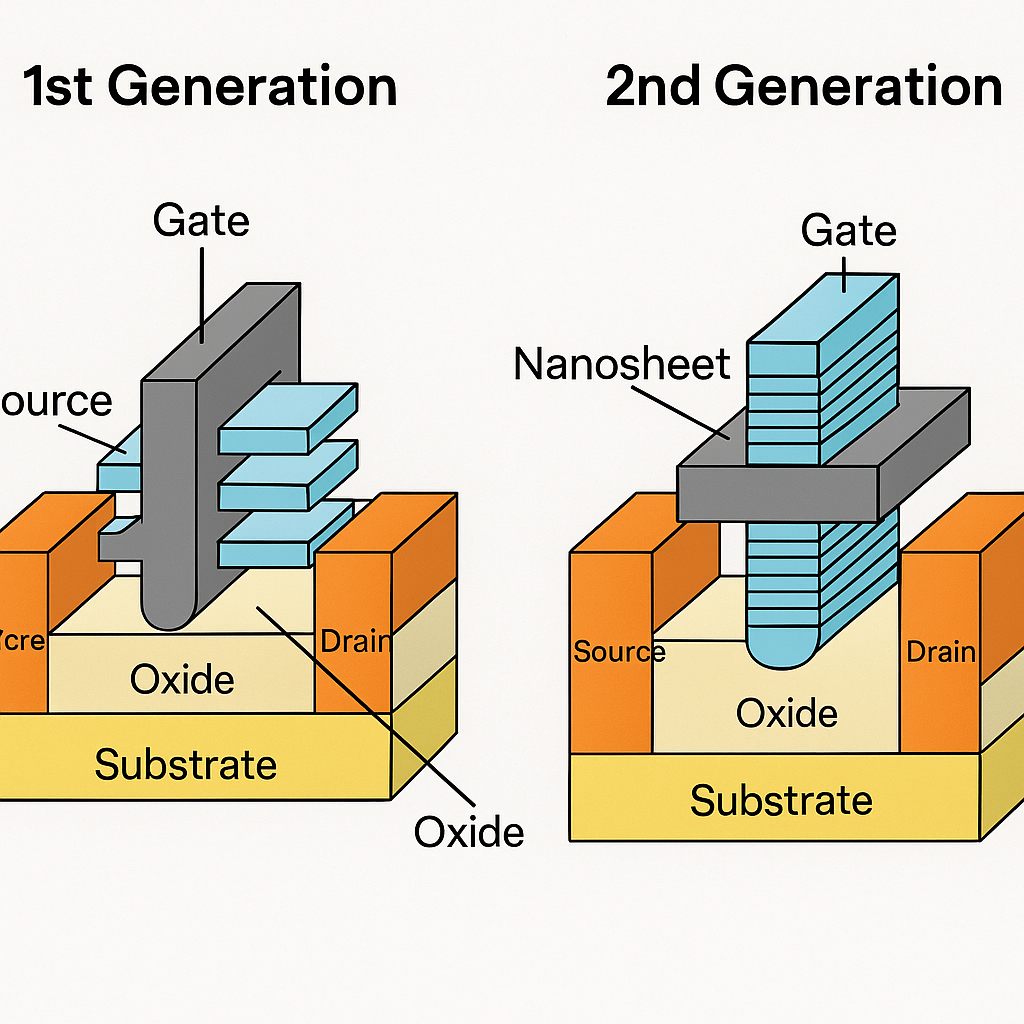
Transistor architecture: 2nd Generation GAAFET (nanosheet)
Backside power variant: A14P (planned for 2029)
Overview
TSMC A14 is the company’s next full-node technology after TSMC N2, representing a significant leap in logic transistor density, power efficiency, and performance. It is built using second-generation Gate-All-Around Field-Effect Transistors (GAAFETs) and is co-optimized with TSMC’s NanoFlex™ Pro architecture to support flexible transistor design across power, performance, and area trade-offs.
Unlike many industry expectations, TSMC will not use High-NA EUV lithography for A14; instead, it continues leveraging its current EUV technology with innovative patterning techniques, thereby reducing cost and complexity.
Process Technology Features
| Feature | Description |
|---|---|
| Node Class | Full node advancement from N2 |
| Transistor Type | 2nd-generation GAAFET (stacked nanosheet) |
| Gate Control | Improved electrostatics over N2; better subthreshold leakage and drive current |
| Lithography | Conventional EUV with advanced multi-patterning |
| NanoFlex Pro Support | Enables per-block transistor width optimization |
| Backside Power (SPR) | Not in base A14; added in A14P variant (2029) |
Performance, Power, and Density (PPA)
Compared to TSMC N2, the A14 node delivers:
-
+10–15% performance gain at the same power
-
– 25–30% power reduction at the same speed
-
+20–23% logic density improvement
These improvements reflect a full node advancement, unlike the intra-node optimizations (e.g., N3E → N3P) seen in previous generations.
Architectural Innovations
◾ 2nd-Gen GAAFETs
TSMC’s A14 transistors benefit from refinements in channel control and nanosheet stacking, allowing tighter pitches, higher drive current, and better leakage characteristics.
◾ NanoFlex™ Pro
An advanced evolution of the original NanoFlex technology used in N2, NanoFlex Pro enables finer-grained transistor width tuning. Designers can choose wider nanosheets for high performance or narrower ones for power efficiency—block by block.
◾ EUV Strategy
TSMC is not adopting High-NA EUV for A14. Instead, it pushes standard NA EUV with more mature multi-patterning and alignment schemes, reducing capital cost and design risk.
Design Ecosystem and IP Readiness
-
EDA and IP partners (Arm, Synopsys, Cadence, etc.) are expected to tape out IP platforms starting 2027.
-
AI accelerators, HPC SoCs, and advanced chiplets will be first to adopt the A14 node.
-
A14 will support 3DIC and chiplet architectures via CoWoS, InFO, and SoIC.
Timeline
| Year | Milestone |
|---|---|
| 2023–24 | A14 announced during TSMC Technology Symposium |
| 2026 | N2P/N2X in production, used as A14 design base |
| 2027 | A14 risk production begins |
| 2028 | A14 enters high-volume manufacturing (HVM) |
| 2029 | A14P variant with backside power delivery (SPR) launches |
Strategic Impact
Industry Leadership
A14 keeps TSMC in the lead for logic process scaling. While Intel plans to introduce 18A (2nm-class) and eventually move to High-NA EUV, TSMC’s more measured approach leverages tool maturity over radical equipment shifts, enabling cost-effective ramp.
AI and HPC Readiness
TSMC positions A14 for AI accelerators, datacenter CPUs, and chiplets, where power density and bandwidth are critical.
Chiplet Integration
A14 will be a key enabler for heterogeneous integration, allowing multiple dies (different nodes and functions) to interconnect with advanced 2.5D/3D packaging.
Beyond A14
TSMC is actively exploring Forksheet FETs and Complementary FETs (CFETs) for post-A14 nodes (e.g., A10 or 1.0nm-class). These may introduce vertical stacking of N- and P-type devices or integration with optical and neuromorphic systems.
Summary
| Feature | TSMC A14 |
|---|---|
| Node Size | ~1.4nm (naming) |
| Transistor Type | 2nd-gen GAAFET |
| Density Gain | +20–23% over N2 |
| Power Reduction | –25–30% |
| Performance Gain | +10–15% |
| EUV Type | Standard NA |
| Backside Power | A14P (2029) |
| High-NA EUV | Not required |
| Volume Production | 2028 |


Captain America: Can Elon Musk Save America’s Chip Manufacturing Industry?