
Also Known As: Semiconductor Industry Supply Chain, Chip Manufacturing Ecosystem
Domain: Electronics, High-Tech Manufacturing, Global Trade
Purpose: To describe the end-to-end ecosystem that enables the design, fabrication, packaging, and delivery of semiconductor chips.
Major Players: EDA vendors, IP providers, Foundries, IDM companies, OSATs, OEMs, Equipment and Materials suppliers
Overview
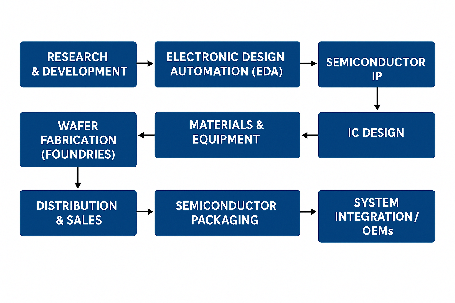
The semiconductor value chain represents the full lifecycle of semiconductor products—from initial design concepts to final integration into electronic systems. This intricate and global ecosystem includes intellectual property (IP) providers, electronic design automation (EDA) vendors, wafer foundries, outsourced semiconductor assembly and test (OSAT) companies, and original equipment manufacturers (OEMs). Each segment plays a crucial role in developing the complex chips that power everything from smartphones and servers to electric vehicles and medical devices.
Key Segments of the Semiconductor Value Chain
1. Research & Development (R&D)
-
Involves fundamental materials science, transistor architecture, and lithography research.
-
Often funded or driven by government labs (e.g., IMEC, SRC, DARPA), universities, and large corporations (e.g., Intel, Samsung, IBM).
2. Electronic Design Automation (EDA)
-
Tools and software used to design complex chips.
-
Functions include logic synthesis, layout, verification, DRC, and power analysis.
-
Major players: Synopsys, Cadence, Siemens EDA (Mentor), Ansys, Empyrean.
3. Semiconductor IP (Intellectual Property)
-
Reusable logic blocks like CPUs, GPUs, SerDes, memory controllers, and security IP.
-
Enables faster design cycles and SoC integration.
-
Key companies: Arm, Imagination, Rambus, Alphawave, CEVA.
4. IC Design
-
Chip companies create schematics, RTL code, and layouts using EDA tools and IP.
-
Two primary business models:
-
Fabless: Design only (e.g., NVIDIA, Qualcomm, AMD)
-
IDM (Integrated Device Manufacturer): Design and manufacture (e.g., Intel, Texas Instruments, Micron)
-
5. Wafer Fabrication (Foundries)
-
Actual manufacturing of chips on silicon wafers in ultra-clean facilities (fabs).
-
Processes involve photolithography, etching, doping, and deposition.
-
Leading pure-play foundries: TSMC, GlobalFoundries, UMC, SMIC.
-
IDM companies with in-house fabs: Intel, Samsung, Micron.
6. Materials & Equipment
-
Equipment includes photolithography machines (e.g., ASML EUV), etchers, metrology tools.
-
Materials include silicon wafers, resists, gases, CMP slurries, and packaging substrates.
-
Major equipment players: ASML, Applied Materials, Lam Research, Tokyo Electron.
-
Materials leaders: Shin-Etsu, SUMCO, DuPont, Merck, JSR.
7. Semiconductor Packaging
-
Assembles dies into usable chips using packages like flip-chip, BGA, or advanced packaging (e.g., CoWoS, Foveros).
-
Involves thermal management, power delivery, and interconnect design.
-
OSAT companies: ASE, Amkor, JCET, SPIL.
-
Also performed in-house by IDMs and some foundries (e.g., TSMC, Intel).
8. Testing
-
Validates that each chip functions correctly before shipment.
-
Includes wafer-level and final packaged IC tests (electrical, thermal, yield).
-
Performed by OSATs or internal test teams using automated test equipment (ATE).
9. Distribution & Sales
-
Chips are shipped to OEMs (Original Equipment Manufacturers), system integrators, and software companies.
-
Distributors like Arrow, Avnet, and WPG facilitate logistics.
10. System Integration / OEMs
-
Final products (e.g., smartphones, laptops, vehicles) are assembled with semiconductor components.
-
Top OEMs: Apple, Samsung, Tesla, Dell, Cisco, Huawei, and many more.
Value Chain Business Models
| Model | Description | Examples |
|---|---|---|
| Fabless | Design only; outsources fabrication | Qualcomm, AMD, MediaTek |
| Foundry | Manufactures for fabless clients | TSMC, UMC, GlobalFoundries |
| IDM | Designs and manufactures chips | Intel, Samsung, Texas Instruments |
| OSAT | Packages and tests chips for others | ASE, Amkor, JCET |
| Design + Foundry Hybrid | Verticalized foundries offering design help | Intel Foundry Services (IFS), Samsung Foundry |
Geographical Distribution
-
Design & IP: USA, UK, Israel, China
-
EDA & Tools: USA-dominated
-
Foundries: Taiwan (TSMC), South Korea (Samsung), China (SMIC)
-
Equipment: Netherlands (ASML), USA, Japan
-
Packaging/Test: Taiwan, China, Malaysia, Singapore
-
OEMs: USA, China, Korea, Japan
Challenges in the Value Chain
-
Geopolitical risk: Trade restrictions and export controls on China
-
Supply chain resilience: COVID and geopolitical disruptions highlighted vulnerabilities
-
Talent shortages: Skilled labor gaps in both engineering and manufacturing
-
Rising cost: Advanced nodes require billions in R&D and capex
Future Trends
-
Advanced packaging (chiplets, 2.5D/3D IC)
-
Vertical integration (e.g., Apple Silicon)
-
Reshoring and regional diversification (CHIPS Act in U.S., Europe’s IPCEI)
-
AI-driven EDA and verification
-
Sustainability and green manufacturing
Conclusion
The semiconductor value chain is a highly interconnected and global ecosystem that underpins nearly all modern technology. Understanding this chain—from design and IP to fabrication, packaging, and system integration—is critical to managing innovation, cost, and risk in the electronics industry. As technologies advance and geopolitical shifts occur, the dynamics within this value chain will continue to evolve.


Chemical Origins of Environmental Modifications to MOR Lithographic Chemistry