Official Names:
-
Samsung 3GAE (3nm Gate-All-Around Early)
-
Samsung 3GAP (3nm Gate-All-Around Plus)
Technology Type: Gate-All-Around (GAA) FET – MBCFET™
Developer: Samsung Electronics (Samsung Foundry)
Announced: 2021 (3GAE), 2022 (3GAP)
Mass Production Start: -
3GAE: June 2022
-
3GAP: Expected 2024–2025
Predecessor: 4nm FinFET
Competitors: TSMC N3B/N3E, Intel 20A
Key Differentiator: First foundry to commercialize GAA transistor architecture at 3nm
Overview
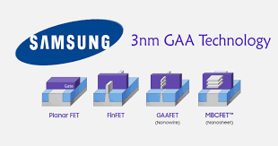
Samsung’s 3nm process node marks a major advancement in semiconductor manufacturing, being the first commercial node to use Gate-All-Around (GAA) transistors—a significant shift from traditional FinFET designs. Branded as MBCFET™ (Multi-Bridge Channel FET), Samsung’s GAA architecture enables greater control over the transistor channel, improved energy efficiency, and enhanced scalability.
Samsung’s 3nm roadmap includes two main versions:
-
3GAE (Early): First generation with reduced performance and yield, primarily for internal and select customers.
-
3GAP (Plus): Enhanced, higher-performance and more stable node aimed at mass production for external customers.
Key Technology: MBCFET™ (Multi-Bridge Channel FET)
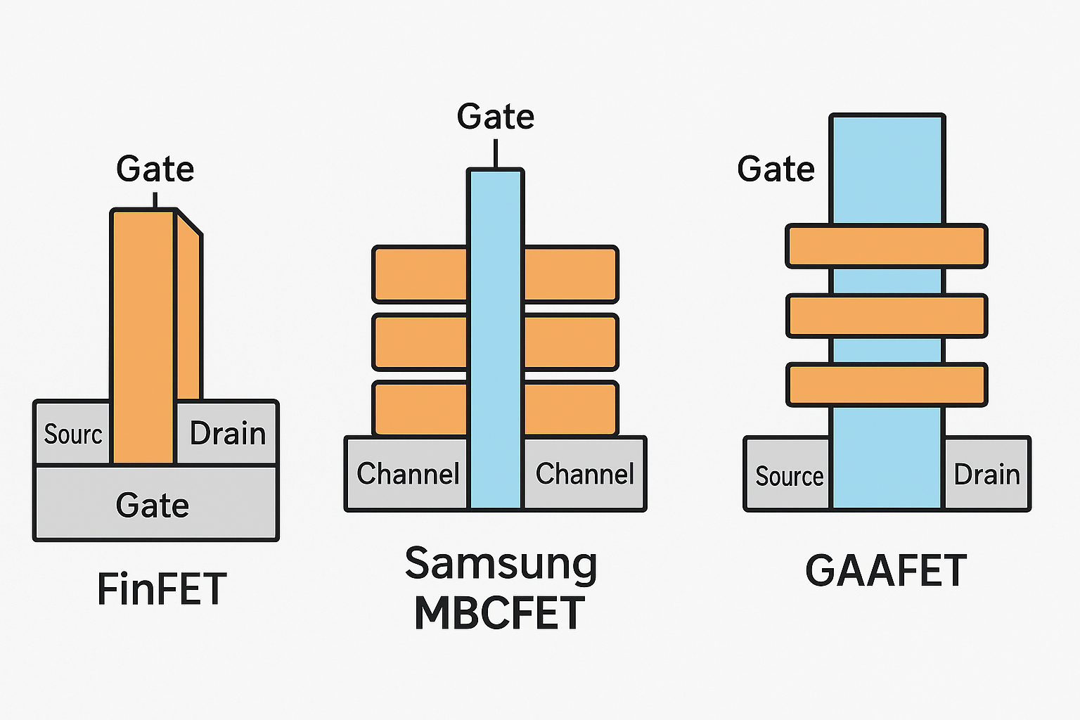
Samsung’s MBCFET is a type of nanosheet GAA transistor where the gate wraps around vertically stacked, flat horizontal channels—similar in concept to a “stacked ribbon.”
Benefits of MBCFET over FinFET:
-
Improved Gate Control: Reduced short-channel effects and leakage.
-
Wider Channel Width Control: Tunable performance and power characteristics by varying sheet width.
-
Better Scaling Potential: Continued Moore’s Law advancement past 5nm.
MBCFET is fully compatible with EUV lithography, enabling dense logic structures with fewer process steps.
Node Performance Metrics
Samsung has provided the following performance improvements for 3GAE vs. 5nm FinFET:
| Metric | Value |
|---|---|
| Power Reduction | Up to 45% |
| Performance Improvement | Up to 23% |
| Area Reduction | Up to 16% |
For 3GAP, these values are expected to improve further:
-
Power reduction: ~50%
-
Performance increase: ~30%
-
Area savings: ~35% over 5nm
Note: Real-world gains depend on chip design and IP integration.
Manufacturing Timeline
| Milestone | Node | Notes |
|---|---|---|
| June 2022 | 3GAE | Samsung begins first GAA-based chip production (limited customers) |
| 2023–2024 | 3GAP risk production | Performance-enhanced version enters risk production |
| 2025 (expected) | 3GAP HVM | Broader foundry customer adoption and volume production |
| Beyond 2025 | SF2 (2nm-class) | Next-generation GAA + BSPDN |
Samsung’s GAA roadmap includes further scaling with SF2, which may integrate backside power delivery (BSPDN) and even CFET stacking technologies in the future.
Design and EDA Ecosystem
Samsung supports the 3nm process with:
-
Foundry Design Kits (FDKs) and PDKs for 3GAE and 3GAP
-
Collaborations with EDA vendors: Synopsys, Cadence, Siemens
-
IP ecosystem partners for memory, interface (e.g., LPDDR5, PCIe), and foundation IP
-
Multi-project wafer (MPW) access for startups and universities
Samsung’s SAFE™ ecosystem (Samsung Advanced Foundry Ecosystem) enables:
-
Physical design tools
-
Simulation, DFT, packaging support
-
Turnkey design services
Applications and Market Segments
Initial 3GAE production has been limited to internal Samsung projects and Chinese cryptocurrency ASICs. 3GAP is targeting a broader range of applications including:
-
Mobile SoCs
-
AI/ML accelerators
-
Networking and datacenter processors
-
Automotive-grade ICs
-
Custom silicon for hyperscalers
Samsung is working to close the yield, power, and performance gap with TSMC, especially for flagship mobile designs and HPC workloads.
Comparison with Competitors
| Feature | Samsung 3GAE | TSMC N3E | Intel 20A |
|---|---|---|---|
| Transistor Type | GAA (MBCFET) | FinFET | GAA (RibbonFET) |
| GAA in Production | ✅ Yes (2022) | ❌ Planned (2025+) | ✅ Risk production (2024) |
| Power Savings (vs 5nm) | ~45% | ~30% | ~25–30% |
| Performance Gain (vs 5nm) | ~23–30% | ~18–20% | ~20% |
| EUV Usage | High | High | High |
| BSPDN | ❌ Not in 3nm | ❌ | ✅ PowerVia |
| Mass Production | 2022 (3GAE), 2025 (3GAP) | 2023 | 2025 (Intel 20A) |
While Samsung leads in early GAA commercialization, Intel and TSMC are planning more aggressive GAA + backside power strategies in upcoming nodes.
Challenges and Criticism
Samsung’s 3GAE rollout faced several hurdles:
-
Low yield and limited customer availability in early production
-
EDA and IP ecosystem lagging behind TSMC’s mature 5nm/3nm stack
-
Customer trust gap due to inconsistent delivery in 4nm node competitiveness
-
Packaging integration and performance for high-performance chiplets still evolving
Samsung’s 3GAP and future nodes aim to resolve these issues and enhance foundry competitiveness.
Strategic Importance
Samsung’s 3nm node is crucial for:
-
Maintaining its position as a leading-edge foundry
-
Demonstrating GAA maturity ahead of rivals
-
Fueling internal SoCs (Exynos, mobile processors)
-
Competing for foundry share in a market increasingly driven by hyperscalers, chiplets, and custom silicon
Conclusion
Samsung’s 3nm (3GAE and 3GAP) node marks a significant milestone as the first commercial implementation of Gate-All-Around transistors using MBCFET. While initial adoption was limited, the improved 3GAP process aims to attract broader foundry customers and push performance boundaries. With competition heating up from Intel and TSMC in the Angstrom era, Samsung’s continued innovation in GAA and advanced packaging will determine its long-term leadership in advanced node manufacturing.


Chemical Origins of Environmental Modifications to MOR Lithographic Chemistry