
Node Name: Samsung 2nm
Internal Name: SF2 (Samsung Foundry 2nm)
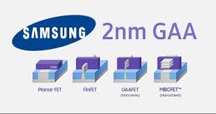
Technology Type: Gate-All-Around (GAA) – MBCFET™
Developer: Samsung Electronics (Samsung Foundry Division)
Announced: May 2022
Targeted Risk Production: 2025
Targeted High Volume Manufacturing (HVM): 2026
Successor to: Samsung 3GAP (3nm Gate-All-Around Plus)
Competitors: TSMC N2, Intel 18A
Key Technology: 2nd generation GAA with improved power and performance, potential backside power integration
Overview
Samsung SF2 (Samsung Foundry 2nm) is Samsung’s next-generation advanced logic process node and the successor to its 3nm process family (3GAE, 3GAP). Continuing the company’s leadership in Gate-All-Around (GAA) transistor technology through MBCFET™ (Multi-Bridge Channel Field-Effect Transistor), SF2 aims to deliver substantial performance and efficiency gains to enable the next era of mobile, AI, HPC, and automotive silicon.
Samsung’s 2nm technology is positioned to compete directly with TSMC’s N2 and Intel’s 18A, both of which also use GAA transistor architectures. Samsung plans to offer SF2 with enhanced nanosheet design, improved power delivery, and possibly backside power delivery (BSPDN) features.
Key Technology: MBCFET 2nd Generation
SF2 uses second-generation MBCFET™ transistors with the following enhancements:
-
Wider and more tunable nanosheets for greater current drive or energy efficiency.
-
Advanced gate stack engineering for better short-channel control.
-
Tighter spacing and improved RC delay optimization for denser logic paths.
-
Lower variability and improved yield potential over 3nm GAA.
Samsung continues to market MBCFET as a superior GAA architecture due to:
-
Scalability of stacked nanosheets
-
Adjustable channel width for performance tuning
-
Improved electrostatics and leakage control
Expected Performance Metrics (vs. 3GAP)
| Metric | Improvement Target |
|---|---|
| Power Efficiency | Up to 25–30% |
| Performance | 10–15% |
| Logic Density | Up to 20% increase |
| Area Scaling | ~15% smaller core sizes |
Note: Final values will depend on library selection, IP maturity, and chip design methodology.
Manufacturing Timeline
| Milestone | Date (Targeted) | Notes |
|---|---|---|
| Announcement | May 2022 | At Samsung Foundry Forum (SFF) |
| R&D Completion | 2024 | Device engineering and PDK qualification |
| Risk Production | Late 2025 | Customer tape-outs begin |
| Volume Ramp | 2026 | Mass production starts |
| Automotive Grade | 2027+ | For ADAS and automotive SoCs |
Design Enablement and IP Ecosystem
Samsung’s SAFE™ Ecosystem supports SF2 with:
-
EDA tools from Synopsys, Cadence, Siemens, and Ansys
-
IP support for Arm cores, LPDDR5/5X, PCIe 6.0, UCIe, and HMB3e
-
PDKs and foundation IP libraries (logic, memory, SRAM, analog)
-
Custom IP porting from 3nm platforms (3GAE/3GAP)
Samsung has also advanced its Advanced Package Integration (API) technologies to complement SF2 with:
-
I-Cube™ (2.5D interposer)
-
X-Cube™ (3D stacked dies)
-
UCIe chiplet support
Target Applications
Samsung SF2 is targeting the most demanding semiconductor segments, including:
-
Mobile SoCs (flagship Exynos and customers)
-
AI/ML accelerators (NPU, DPU, inference engines)
-
High-performance computing (HPC) chips
-
Automotive processors (ADAS, autonomous driving)
-
Datacenter and cloud compute infrastructure
Comparison with Competitors
| Feature | Samsung SF2 | TSMC N2 | Intel 18A |
|---|---|---|---|
| Transistor | MBCFET (GAA) | Nanosheet GAA | RibbonFET (GAA) |
| Backside Power | Possible in SF2P/SF2GAP | Yes (BSPDN) | Yes (PowerVia) |
| Gate Pitch | ~44–48nm (estimated) | ~45nm | ~44nm |
| First Production | 2025 (risk), 2026 (HVM) | 2025 | 2025 |
| Ecosystem Maturity | Developing | Very mature | Improving rapidly |
| Packaging Options | I-Cube, X-Cube | CoWoS, SoIC | Foveros, EMIB |
Samsung is currently second in the foundry market behind TSMC, and SF2 is critical to expanding its competitiveness, especially in advanced logic and AI markets.
Challenges
Samsung faces multiple hurdles with SF2:
-
Tooling yield optimization for second-gen MBCFET devices
-
EDA and IP maturity compared to TSMC
-
High mask costs and EUV tool dependency
-
Customer trust and design enablement gaps due to previous 4nm/3nm execution delays
-
Field size and stitching if advanced patterning (High-NA EUV) is delayed
Strategic Importance
SF2 is a linchpin in Samsung’s:
-
Technology leadership strategy in GAA and advanced packaging
-
Competition with TSMC and Intel for leading-edge logic and AI chips
-
Expansion into automotive and AI markets where power/performance leadership is critical
-
Vision for 1.4nm and below, where MBCFET scalability and BSPDN become essential
Outlook and Beyond
Samsung plans to follow SF2 with:
-
SF2P (Performance-enhanced)
-
SF2GAP (possibly with backside power)
-
SF1.4 (1.4nm node) – around 2027–2028, expected to introduce CFET or vertical transistors
Samsung has also confirmed High-NA EUV adoption after 2026, likely aligning with SF1.4 and beyond.
Conclusion
Samsung’s 2nm process node (SF2) is a pivotal advancement in the foundry race, continuing the evolution of GAA technology with MBCFET and laying the groundwork for next-generation AI, mobile, and high-performance chips. While it faces stiff competition from TSMC’s N2 and Intel’s 18A, SF2’s success will hinge on execution, customer enablement, and ecosystem growth over the next few years.


Things From Intel 10K That Make You Go …. Hmmmm