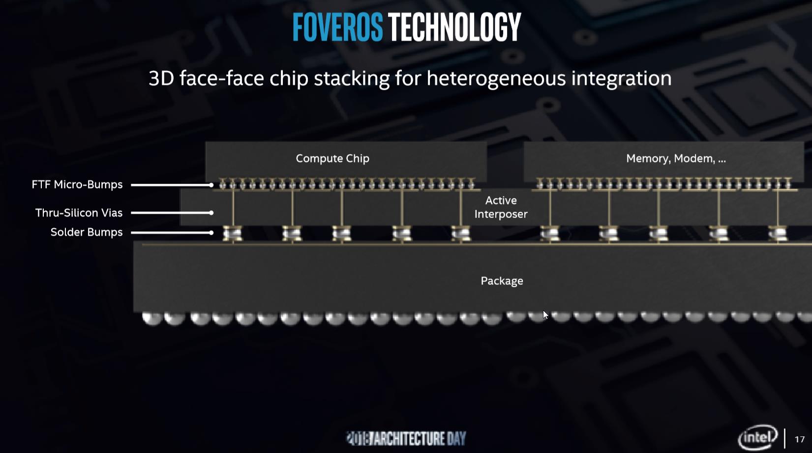


Foveros is a 3D chip stacking technology developed by Intel that enables high-density vertical integration of multiple active logic dies using face-to-face (F2F) hybrid bonding and through-silicon vias (TSVs). First unveiled in December 2018, Foveros allows for heterogeneous integration of compute, graphics, AI, and IO chiplets on top of a base die, unlocking new architectural flexibility, power efficiency, and form factor innovation.
As part of Intel’s advanced packaging portfolio—which also includes EMIB (Embedded Multi-die Interconnect Bridge) and ODI (Omni-Directional Interconnect)—Foveros is a key pillar in Intel’s IDM 2.0 strategy and central to products built with disaggregated SoC architectures such as Meteor Lake, Arrow Lake, and Ponte Vecchio.
Overview
Foveros uses 3D die stacking to vertically integrate a smaller logic chiplet (tile) on top of a larger base die (typically used for IO, power delivery, or memory). Unlike passive interposers in 2.5D packaging (e.g., CoWoS or EMIB), Foveros enables active logic-on-logic stacking, making it ideal for compact, power-sensitive designs such as mobile processors and AI accelerators.
By enabling each die to be fabricated on different process nodes, Foveros supports heterogeneous integration, allowing designers to mix high-performance cores, low-power cores, analog/RF functions, and accelerators in a flexible manner.
Key Features
| Feature | Description |
|---|---|
| 3D Stacking | Logic-on-logic die stacking via TSVs and hybrid bonding |
| Heterogeneous Integration | Mix different process nodes and functions (CPU, GPU, AI, IO) |
| Power Efficiency | Fine-grained power management and reduced interconnect lengths |
| Compact Footprint | Enables ultra-thin, mobile-friendly package form factors |
| Node Flexibility | Top and base dies can be made in different fabs/processes |
| Reusability | Base dies can be reused across multiple product SKUs |
How Foveros Works
-
A base die is manufactured with support logic, power delivery, and TSVs.
-
A logic tile (chiplet) is manufactured separately—typically containing high-performance compute blocks.
-
The logic die is bonded face-to-face on top of the base die using hybrid bonding.
-
Power and signal routes pass vertically via fine-pitch micro-bumps and TSVs in the base die.
-
Additional chiplets (e.g., GPU, AI, memory tiles) can be integrated horizontally via EMIB or ODI.
Foveros Products and Use Cases
Meteor Lake (Intel Core Ultra)
-
Intel’s first disaggregated client SoC
-
Combines CPU, GPU, SoC, and IO tiles using Foveros
-
Manufactured on Intel 4 and TSMC N5 nodes
-
Enabled Intel’s chiplet strategy for mobile and desktop
Ponte Vecchio / Intel Max GPU
-
Intel’s flagship HPC GPU
-
Over 47 tiles connected via Foveros + EMIB
-
Combines tiles from Intel, TSMC, and third-party fabs
Lakefield
-
First commercial Foveros product (2019)
-
Hybrid x86 + Atom CPU architecture for ultra-mobile devices
Future Roadmap
-
Arrow Lake, Lunar Lake, and Panther Lake will extend Foveros usage
-
Foveros will play a central role in AI PCs, low-power edge designs, and HPC accelerators
Foveros vs. Other Technologies
| Feature | Foveros | EMIB | TSMC SoIC | TSMC CoWoS | Samsung X-Cube |
|---|---|---|---|---|---|
| Type | 3D | 2.5D | 3D | 2.5D | 3D |
| TSVs | Yes | No | Yes | Yes | Yes |
| Stacking | Logic on logic | Side-by-side | Face-to-face | Side-by-side | Face-to-face |
| Thermal Mgmt | Challenging | Easier | Complex | Easier | Complex |
| Bandwidth | Very High | High | Ultra High | High | High |
| Integration | Vertical | Horizontal | Vertical | Horizontal | Vertical |
Technical Innovations
-
Fine-pitch hybrid bonding (~10μm and shrinking)
-
Ultra-low z-height for thin form factors
-
Advanced power delivery networks (PDNs) through base die
-
Die-to-die link tuning with power and latency optimization
-
Thermal-aware floorplanning to mitigate hot spot stacking
Challenges
-
Thermal management for stacked dies (especially in mobile/HPC)
-
Yield sensitivity to base die and logic die defects
-
Design complexity and EDA co-design requirements
-
TSV density and die thinning need precise control
-
Packaging cost compared to monolithic SoCs
Future Directions
-
Scaling to <10μm bonding pitch and hybrid direct bonding
-
Integration of SRAM, DRAM, photonics, and AI engines in 3D stacks
-
Foveros Omni and Foveros Direct:
-
Foveros Omni: Flexible 3D stacking with increased customization
-
Foveros Direct: Direct copper-to-copper bonding for lower resistance
-
-
Co-packaged optics, chiplet marketplaces, and UCIe-compliant 3D systems
Foveros and UCIe
-
Intel is a founding member of the UCIe (Universal Chiplet Interconnect Express) consortium
-
Foveros complements UCIe by enabling 3D stacking while UCIe governs die-to-die protocols
-
Intel’s open ecosystem strategy enables customers to use Foveros with UCIe-compliant chiplets
Also Read:
Share this post via:


Silicon Insurance: Why eFPGA is Cheaper Than a Respin — and Why It Matters in the Intel 18A Era