

Name: PowerVia™
Type: Backside Power Delivery Network (BSPDN)
Developer: Intel Corporation
First Production Node: Intel 20A (2nm-class)
Announced: July 2021
Expected Production Deployment: 2024 (Intel 20A), with high-volume in 2025
Successor Technologies: Integrated with RibbonFET (Intel’s Gate-All-Around)
Competes With: TSMC’s back-side power roadmap, Samsung’s BSPDN research initiatives
Overview
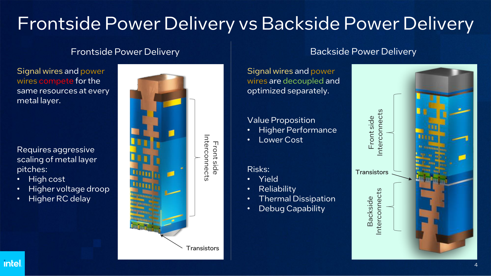
PowerVia™ is Intel’s proprietary Backside Power Delivery Network (BSPDN) technology, designed to improve transistor performance, reduce power losses, and optimize signal routing. PowerVia marks Intel’s transition from traditional front-side power delivery to a groundbreaking backside approach, where power rails are routed beneath the silicon substrate, freeing up the front side for signal wiring.
PowerVia is part of Intel’s Intel 20A process node, which also introduces RibbonFET, the company’s first gate-all-around (GAA) transistor design. These innovations together enable continued scaling beyond FinFET, as Moore’s Law progresses into the angstrom era.
What is Backside Power Delivery?
In conventional semiconductor design, both power (VDD/GND) and signal interconnects are routed through multiple layers on top of the silicon wafer. As transistors scale down and routing density increases, this front-side configuration causes:
-
Increased routing congestion
-
Voltage droop and IR drop
-
Reduced power efficiency
-
Difficulties in meeting signal integrity and performance targets
Backside Power Delivery solves this by moving the power routing beneath the transistor layer, separating the power and signal networks. This decouples signal integrity from power constraints and opens new optimization opportunities for device and circuit designers.
How PowerVia Works
Key Features:
-
Backside Metal Layers: Power lines (VDD and GND) are routed on the bottom of the silicon substrate.
-
Through-Silicon Vias (TSVs): Used to connect backside power rails to the transistor layers above.
-
Front-Side Reserved for Signals: All signal routing now happens above the transistors, with more space and less interference.
This approach is similar in concept to 3D packaging techniques, but applied at the transistor-level. Intel is the first major manufacturer to bring backside power into mass production at scale.
Benefits of PowerVia
PowerVia delivers several key advantages for advanced nodes:
| Benefit | Description |
|---|---|
| Increased Performance | Reduced IR drop and improved power delivery allow transistors to operate at higher speeds. |
| Improved Power Efficiency | Dedicated power routing improves voltage stability and reduces parasitic losses. |
| Signal Routing Simplification | Signal interconnects face less congestion and interference. |
| Smaller Cell Footprint | Freed-up front-side metal layers allow for tighter standard cell packing. |
| Enabler for RibbonFET | Facilitates the use of Intel’s new GAA transistors (RibbonFET) by reducing electromigration and noise issues. |
Intel reports >6% performance gain at iso-power compared to front-side power networks, and a better overall power-performance-area (PPA) trade-off than previous nodes.
Implementation Timeline
| Node | Year | Technology | Status |
|---|---|---|---|
| Intel 20A | 2024 | PowerVia + RibbonFET | First production deployment |
| Intel 18A | 2025 | Optimized PowerVia | High-volume manufacturing |
| Intel 14A and beyond | 2026–2027+ | Advanced BSPDN + GAA enhancements | In research and pathfinding |
PowerVia was first demonstrated in test silicon in 2022, and successfully validated in Intel’s internal Intel 4 node test vehicles. Early integration results guided its deployment in Intel 20A, targeted at flagship CPU and custom silicon products.
Comparison to Other Approaches
Intel vs. TSMC vs. Samsung
| Feature | Intel (PowerVia) | TSMC | Samsung |
|---|---|---|---|
| BSPDN in Production | Yes (2024) | Roadmap (2025–2026) | In research phase |
| First Node | Intel 20A | Possibly N2 | TBD |
| GAA Integration | RibbonFET + PowerVia | Nanosheet (TSMC N2) | MBCFET (3nm+) |
| Ecosystem Tools | Intel UDP, IFS Accelerator | Mature | Moderate |
| Foundry Offering | Yes (IFS) | Yes (via TSMC) | Yes |
Intel is ahead of its peers in BSPDN manufacturing readiness, and PowerVia gives it a strategic edge in chip power efficiency, especially for high-performance computing (HPC) and AI accelerators.
Applications and Impact
1. Intel Products
-
Intel 20A & 18A CPUs: Next-gen Core and Xeon processors will feature PowerVia for improved performance-per-watt.
-
AI & Graphics: Accelerated computing chips will benefit from reduced thermal and power bottlenecks.
-
Edge & IoT: Improved efficiency in constrained environments.
2. Intel Foundry Services (IFS)
-
External customers targeting HPC, automotive, and defense markets can leverage PowerVia via IFS offerings.
-
IP enablement through IFS Accelerator ecosystem.
3. Industry Implications
-
Sets a precedent for BSPDN as a required technology for future scaling.
-
Forces competitors to accelerate their own backside power roadmaps.
-
Opens new avenues for co-optimization of silicon, packaging, and chiplet integration.
Challenges
Despite its advantages, PowerVia introduces technical hurdles:
-
Manufacturing Complexity: Requires backside wafer thinning, TSV formation, and dual-side processing.
-
EDA Tooling: Demands new CAD tools and PDKs that account for dual-routing layers and thermal constraints.
-
Design Migration: Engineers must adopt new design rules, especially for power domains and IR drop analysis.
Intel has worked closely with EDA vendors and internal toolchains to ensure PowerVia is manufacturable and designer-accessible.
Conclusion
Intel’s PowerVia is a landmark innovation in advanced semiconductor manufacturing, enabling better power efficiency, performance scaling, and transistor density in a post-FinFET world. As the industry approaches the limits of traditional front-side scaling, backside power delivery is expected to become a mainstay of advanced nodes.
Intel’s first-to-market execution with PowerVia demonstrates its technological leadership, reinforces its IDM 2.0 strategy, and positions it as a leading foundry and product provider in the angstrom era.


Silicon Insurance: Why eFPGA is Cheaper Than a Respin — and Why It Matters in the Intel 18A Era