
Overview
Intel 7 is a 10nm-class semiconductor manufacturing node developed by Intel Corporation, first announced in July 2021 as part of the company’s updated process node naming scheme. Despite its name, Intel 7 is not a 7nm node by conventional industry standards, but rather an enhanced version of Intel’s previous 10nm SuperFin node. It offers improved performance-per-watt and transistor density through refined process optimizations and additional EUV (extreme ultraviolet) lithography.
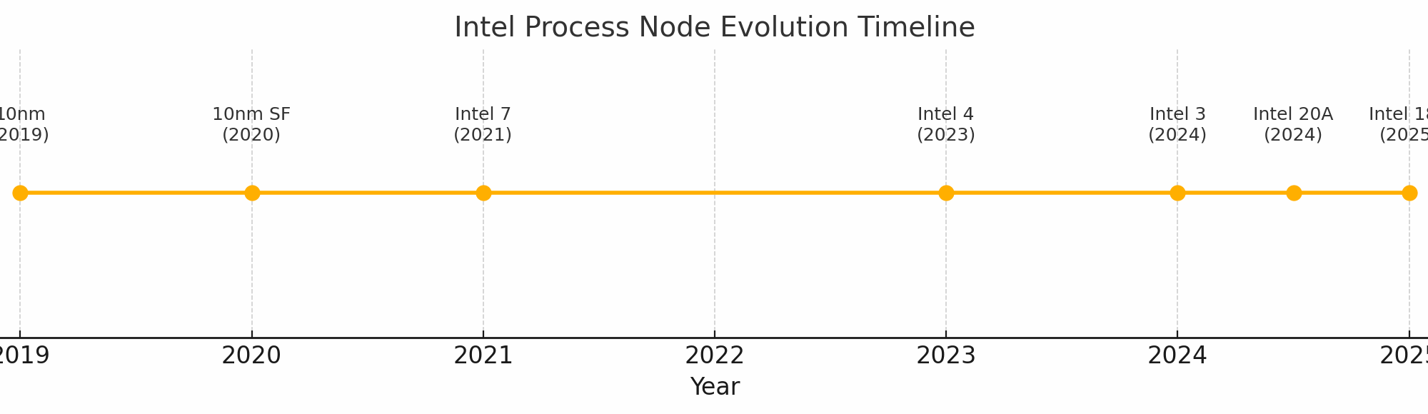
Intel 7 was the first node in the company’s roadmap that aligned with its “Intel Accelerated” strategy, marking the beginning of a new era in its manufacturing comeback.
Key Specifications
| Feature | Intel 7 |
|---|---|
| Node Class | Enhanced 10nm |
| Launch Year | 2021 (products in 2022) |
| Transistor Type | FinFET |
| Lithography | DUV + limited EUV |
| Density Gain | ~10–15% vs. 10nm SuperFin |
| Performance/Watt | +10–15% |
| Products | Alder Lake, Raptor Lake CPUs |
| Fab Locations | Intel D1X (Oregon), Arizona |
Technical Enhancements
Intel 7 is an evolution of 10nm SuperFin, rather than a brand-new node. Improvements include:
-
More mature FinFET architecture with tighter design rules.
-
Enhanced SuperMIM capacitors for better transistor switching.
-
Increased drive current for improved logic performance.
-
Optimizations in metal stack and contact resistance to reduce power.
Although the node still relies mostly on deep ultraviolet (DUV) lithography, it introduces early EUV layers, paving the way for Intel’s transition to future nodes like Intel 4 and Intel 3, which feature more extensive EUV use.
Naming Clarification
Intel rebranded its nodes in July 2021 to better align with industry naming conventions. Under the old naming:
-
Intel 7 ≈ Enhanced 10nm SuperFin
-
Intel 4 ≈ Formerly 7nm
-
Intel 3 ≈ Enhanced Intel 4
This adjustment was designed to more accurately reflect transistor performance and density relative to competitors like TSMC N7/N5 and Samsung 7nm EUV.
Products Based on Intel 7
Client Processors
-
Alder Lake (12th Gen Core, 2021–2022): Intel’s first hybrid architecture with Performance and Efficiency cores (P-cores & E-cores).
-
Raptor Lake (13th Gen Core, 2022–2023): Evolution of Alder Lake with more E-cores and improved cache.
Data Center
-
Sapphire Rapids Xeon Scalable CPUs: Initially delayed, eventually launched in 2023 using Intel 7 for AI, HPC, and cloud workloads.
-
Integrated HBM variants and accelerator blocks (AMX, DSA, IAA) leveraged Intel 7’s performance-per-watt improvements.
Competitive Positioning
At the time of launch, TSMC’s N5 and Samsung’s 5nm EUV were already in high-volume production. While Intel 7 lagged in transistor density (estimated ~90 MTr/mm² vs. TSMC N5’s 130 MTr/mm²), it made up ground in performance and power efficiency, especially in high-frequency workloads and multi-core scaling.
Intel 7 was not EUV-based at scale, limiting density improvements, but the refined FinFETs allowed Intel to remain competitive in client PCs and certain server segments.
Manufacturing and Scaling
-
Fabricated at Intel’s U.S. fabs, primarily D1X in Oregon and Fab 42 in Arizona.
-
Intel 7 was designed with forward compatibility to Intel 4, easing migration to EUV-centric nodes.
-
Marked the company’s return to a yearly cadence of process improvement, setting the stage for Intel 4, Intel 3, Intel 20A, and Intel 18A.
Legacy and Roadmap Role
Intel 7 served as a crucial bridge node, stabilizing Intel’s manufacturing roadmap after delays in 10nm and 7nm. It:
-
Proved Intel could deliver competitive client and server CPUs with improved efficiency.
-
Supported the first modern hybrid core architecture in PCs.
-
Paved the way for EUV adoption and new transistor designs (RibbonFET, PowerVia) in Intel 20A/18A.


Chemical Origins of Environmental Modifications to MOR Lithographic Chemistry