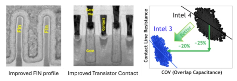
Node Name: Intel 3
Process Class: 3nm (Intel naming)
Technology Type: FinFET (last FinFET node before transition to GAA)
Announced: July 2021 (as part of Intel’s process roadmap)
Production Start: Late 2023 (initial ramp), volume production in 2024
Primary Use Cases: Data center, high-performance computing (HPC), networking, custom silicon
Successor: Intel 20A (2nm-class, GAA)
Competes With: TSMC N3B/N3E, Samsung 3GAE/3GAP
Overview
Intel 3 is a semiconductor manufacturing process developed by Intel Corporation as part of its rebranded and restructured process roadmap introduced in 2021. Despite the “3” in the name, Intel 3 does not refer to a 3nm physical gate length; instead, it is a marketing node name equivalent in class to TSMC’s N3 and Samsung’s 3nm nodes.
Intel 3 is an enhanced refinement of Intel 4 (Intel’s first EUV node), providing higher performance-per-watt, denser logic, and expanded design flexibility while still using FinFET transistor architecture. It is the last node before Intel transitions to its next-generation RibbonFET (gate-all-around) technology on Intel 20A.
Key Technical Features
-
FinFET Transistors: Maintains the tried-and-tested FinFET design with enhancements to boost performance and density.
-
EUV Lithography: Uses more extensive EUV layers than Intel 4 to simplify the process, reduce mask counts, and improve fidelity.
-
Performance Gain: Up to 18% higher performance-per-watt compared to Intel 4 (at iso power).
-
Density Improvements: Slight logic scaling improvement over Intel 4, primarily through tighter cell libraries and improved routing.
-
Metal Stack Enhancements: Improved interconnect delay and power with advanced metallization.
-
Library and IP Availability: Supports a broader range of voltage thresholds, increased mix of standard cells, and more mature IP ecosystem.
Development History
Intel 3 was first revealed in July 2021, when CEO Pat Gelsinger restructured Intel’s process naming to align more clearly with industry terminology. Intel abandoned its prior naming conventions (e.g., 10nm Enhanced SuperFin) and introduced a new roadmap:
-
Intel 7 (formerly 10nm Enhanced SuperFin)
-
Intel 4 (first EUV node)
-
Intel 3 (refined EUV and FinFET)
-
Intel 20A (GAA + backside power)
-
Intel 18A (enhanced GAA + PowerVia)
Originally scheduled for H2 2023 ramp, Intel 3 entered early risk production on schedule, with volume production and commercial products expected by mid-2024.
Applications and Product Use
Intel 3 is targeted primarily at data center and infrastructure products, particularly within Intel’s Xeon server roadmap:
-
Granite Rapids: Next-generation Xeon Scalable processors using Intel 3.
-
Custom Foundry Projects: Intel 3 is one of the initial nodes offered via Intel Foundry Services (IFS) to external customers.
Other potential uses include:
-
Networking ASICs
-
Edge and AI accelerators
-
Defense-grade semiconductors (through U.S. government partnerships)
-
Infrastructure and telecom SoCs
Foundry Offering and IP Ecosystem
As part of Intel Foundry Services (IFS), Intel 3 is available to external customers, complete with:
-
EDA tool enablement from Cadence, Synopsys, Ansys, Siemens
-
Design libraries for digital logic, analog/mixed-signal, high-speed SerDes, and memory IP
-
Support for advanced packaging via EMIB and Foveros
-
Process Design Kits (PDKs) for external customers, including support for UCIe-based chiplets
Intel also offers customization of power-performance tradeoffs, suitable for both high-frequency and low-leakage applications.
Comparison to Competing Nodes
| Feature | Intel 3 | TSMC N3E | Samsung 3GAE |
|---|---|---|---|
| Transistor Type | FinFET | FinFET | GAA (early MBCFET) |
| EUV Usage | High | Moderate | High |
| Density Gain (vs prior) | ~5-10% over Intel 4 | ~1.7x vs N5 | ~1.35x vs 5nm |
| Performance Boost | ~18% over Intel 4 | ~10% vs N5 | ~20% vs 5nm |
| Risk Production | Late 2023 | 2022–2023 | 2022 (limited) |
| Volume Production | 2024 | 2024 | 2024 |
| Ecosystem Maturity | Growing | Very Mature | Moderate |
Intel 3 is a transitional node offering enhanced maturity and yield stability compared to early EUV nodes. While TSMC’s N3E is widely adopted by Apple and AMD, Intel 3 is still gaining momentum among foundry customers.
Status and Adoption (as of 2025)
-
Intel 3 has reached high-yield production and is being used in pre-qualification for Granite Rapids and related Xeon series chips.
-
Select IFS customers have started tape-outs using Intel 3 for custom AI, automotive, and defense applications.
-
The design ecosystem continues to expand with PDK and IP improvements across multiple tool vendors.
Strategic Importance
Intel 3 plays a crucial role in:
-
Bridging the gap between Intel’s FinFET legacy and its upcoming RibbonFET (GAA) nodes.
-
Demonstrating Intel’s renewed manufacturing execution under IDM 2.0.
-
Validating IFS capabilities for delivering foundry services to external partners.
-
Supporting national semiconductor security goals in alignment with the CHIPS and Science Act.
Conclusion
Intel 3 marks a significant step forward in Intel’s process technology roadmap, combining robust FinFET performance with EUV efficiency and a broader design ecosystem. As Intel prepares for its transition to gate-all-around with Intel 20A and 18A, Intel 3 stands as a key production node for current high-performance applications, reaffirming Intel’s capability to deliver competitive, high-volume manufacturing solutions.
Share this post via:


Captain America: Can Elon Musk Save America’s Chip Manufacturing Industry?