

Intel 18A(P) (also referred to as Intel 18A+ or simply 18A Performance) is Intel’s upcoming advanced semiconductor process node, positioned as a refinement and performance enhancement of the base Intel 18A node. It marks a critical step in Intel’s roadmap to reclaim process leadership by the latter half of the 2020s, leveraging RibbonFET (Intel’s implementation of gate-all-around FETs) and PowerVia, a novel back-side power delivery architecture.
Overview
-
Node Name: Intel 18A(P)
-
Estimated HVM (High Volume Manufacturing): Late 2025 to early 2026
-
Target Markets: High-performance computing (HPC), AI accelerators, datacenter CPUs, advanced foundry customers
-
Fabs: Primarily at Intel’s D1X Mod3 (Oregon), Fab 52/62 (Arizona), and potentially Ohio (2026+)
Key Technology Features
| Feature | Description |
|---|---|
| RibbonFET | Intel’s GAA transistor with nanosheet architecture. Provides better electrostatic control and scalability beyond FinFET. |
| PowerVia | Intel’s backside power delivery. Improves performance and reduces IR drop by separating power and signal routing layers. |
| High-κ/Metal Gate | Enhanced for ultra-thin gate oxide control. |
| EUV Lithography | NA |
| Smart Metal Stack | Optimized BEOL (back end of line) with improved RC delay and thermal characteristics. |
| Design Enablement | Includes support for Intel’s Internal Design Teams and IFS (Intel Foundry Services) ecosystem customers. |
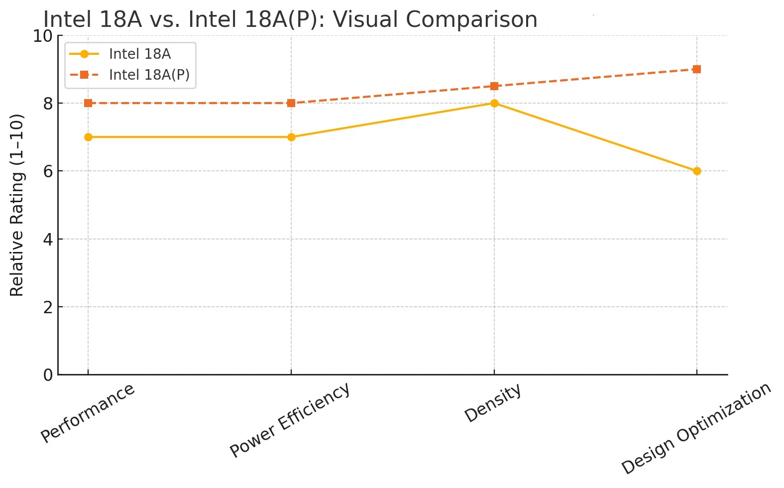
Performance Metrics (Projected)
| Metric | Base 18A vs. 18A(P) |
|---|---|
| Performance | Up to 10–15% higher (clock speed or IPC improvements) |
| Power Efficiency | ~10% better energy efficiency (at iso-performance) |
| Density | Slight improvements due to transistor tuning and interconnect optimizations |
These figures are estimated; Intel has not disclosed full 18A(P) PPA metrics as of mid-2025.
Manufacturing Readiness
-
High-NA EUV Integration:
18A(P) is one of the first nodes globally expected to use ASML’s High-NA EUV (0.55 NA) scanners in production, starting with limited layers. -
Internal Test Chips:
Intel has confirmed that test chips for 18A+ have been successfully taped out and evaluated with internal toolchains. -
Foundry Customers:
Intel Foundry Services (IFS) has signed major customers, including reports of ARM-based and RISC-V core development on 18A and 18A(P).
Design Enablement & IP
-
EDA Tool Support:
Collaborations with Synopsys, Cadence, Siemens EDA, and Ansys for certified flows. -
Standard Cell Libraries:
Intel is offering standard logic cell libraries and memory compilers for external customers. -
IP Portfolio:
Includes SRAM, SerDes, PCIe, DDR, HBM, and AI accelerators co-optimized for 18A(P).
Evolutionary Path
🔹 Intel 20A
-
First RibbonFET + PowerVia
-
Expected HVM: 2024 (Intel Core Ultra 200V “Arrow Lake”)
🔹 Intel 18A
-
Second-gen RibbonFET and PowerVia
-
HVM: 2H 2025 (Intel Clearwater Forest and IFS customers)
🔹 Intel 18A(P) (this node)
-
Performance-enhanced version of 18A
-
Optimized transistor tuning, EUV-based design rules
-
Late 2025 / early 2026 HVM
🔹 Intel 14A (Speculative)
-
Potential next node post-18A(P), possibly integrating advanced 2D materials or stacked nanosheets. Possible use of High-NA EUV.
Timeline
| Year | Milestone |
|---|---|
| 2023 | Intel announces test silicon and 18A tapeouts |
| 2024 | Intel 20A enters limited production |
| 2025 (H1) | 18A qualification and ramp |
| 2025 (H2) | 18A(P) early production with High-NA EUV |
| 2026 | IFS customer delivery for 18A(P) begins |
Strategic Significance
-
Competitive Position: Intel 18A(P) is Intel’s bid to leapfrog TSMC’s A16 and Samsung’s SF2, especially for compute-intensive and AI-dense workloads.
-
Foundry Vision: A cornerstone of Intel’s “Five Nodes in Four Years” strategy and its ambition to become the #2 foundry by 2030.
-
Customer Impact: May power advanced AI, RISC-V, and custom hyperscaler silicon with a focus on tight transistor-channel control and power delivery efficiency.


Captain America: Can Elon Musk Save America’s Chip Manufacturing Industry?