

Node Name: Intel 18A
Process Class: ~1.8nm (Angstrom-class node)
Announced: July 2021
First Production Tapeout: Late 2024 (risk production)
High-Volume Manufacturing: Expected in 2025
Transistor Type: RibbonFET (Gate-All-Around)
Power Delivery: PowerVia (Backside Power Delivery Network)
Foundry Availability: Yes (via Intel Foundry Services – IFS)
Successor Node: Intel 14A (in development)
Competitors: TSMC N2, Samsung 2nm-class (SF2/2GAP)
Overview
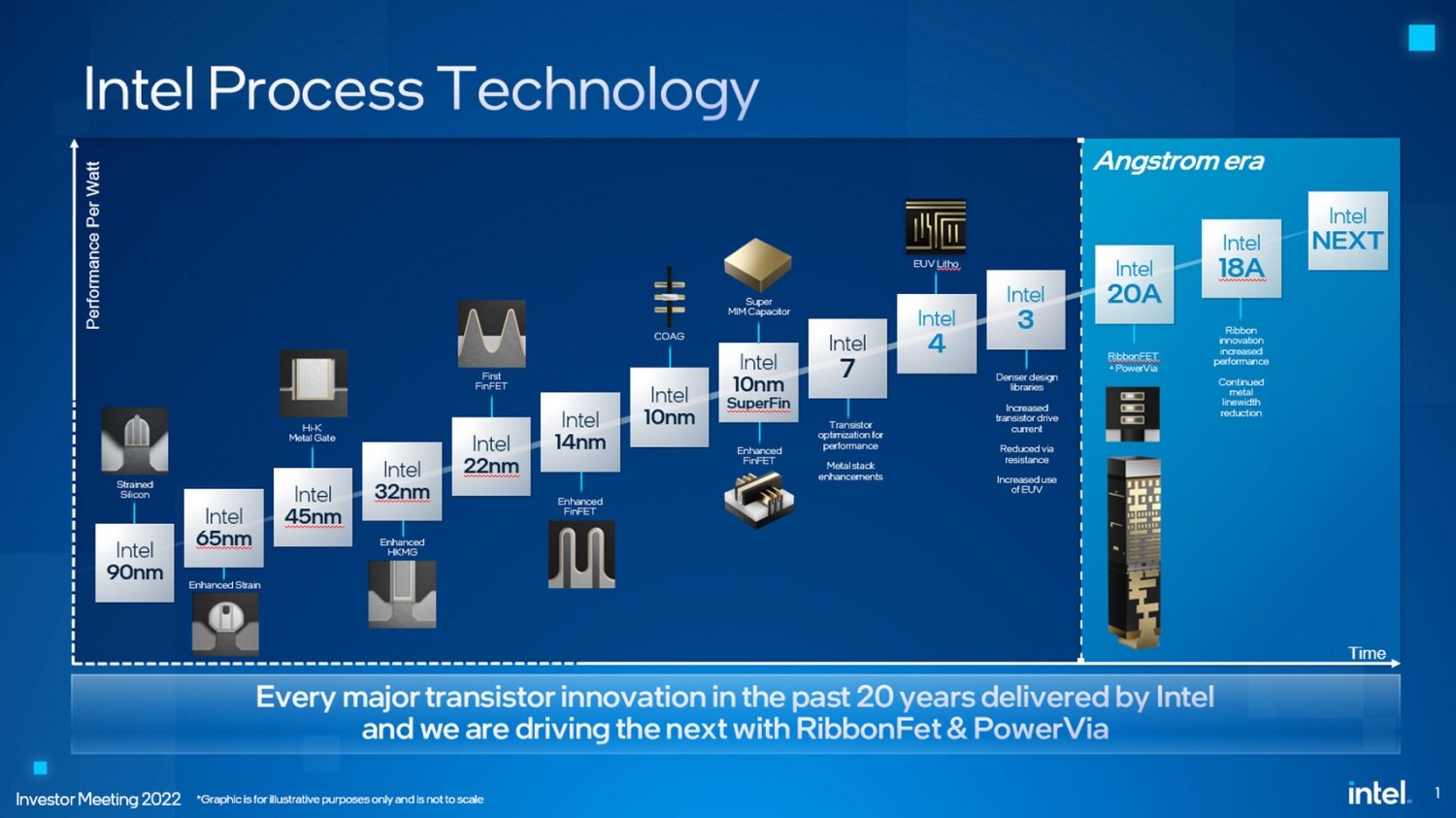
Intel 18A (short for “1.8 Angstroms”) is an advanced Angstrom-class semiconductor manufacturing process node developed by Intel Corporation. It represents one of the most significant technological leaps in Intel’s history, combining next-generation RibbonFET transistors with PowerVia, the industry’s first backside power delivery network (BSPDN) in high-volume production.
Intel 18A is positioned as the second “Angstrom node” in Intel’s redefined roadmap (after Intel 20A), targeting high-performance computing (HPC), AI, and foundry customers. Intel has claimed 18A will deliver performance-per-watt leadership over competing nodes from TSMC and Samsung.
Naming and Node Evolution
Intel rebranded its node naming system in July 2021 to better align with industry trends and customer expectations:
| Legacy Name | New Name | Key Technology |
|---|---|---|
| 7nm | Intel 4 | First EUV |
| n/a | Intel 3 | Enhanced EUV + FinFET |
| n/a | Intel 20A | RibbonFET + PowerVia (2024) |
| n/a | Intel 18A | Enhanced RibbonFET + Optimized PowerVia (2025) |
Although the “18A” name implies 1.8Å, this is a marketing term and does not directly correspond to physical gate length. It places Intel in the same generation as TSMC’s N2 (2nm) and Samsung’s SF2.
Key Technologies in Intel 18A
1. RibbonFET (Gate-All-Around Transistor)
-
Intel’s first gate-all-around (GAA) transistor, and its first new transistor architecture since FinFET in 2011.
-
RibbonFET wraps the gate entirely around the conducting channel, improving electrostatic control, reducing leakage, and enabling shorter gate lengths.
-
Delivers higher drive current and better scalability for dense and high-performance designs.
2. PowerVia (Backside Power Delivery Network)
-
PowerVia moves power delivery to the backside of the wafer, separating it from signal routing.
-
Reduces IR drop, improves signal integrity, and enables denser routing on the front side.
-
Intel 18A features an optimized PowerVia over the version used in Intel 20A.
3. High EUV Integration
-
Uses extensive extreme ultraviolet (EUV) lithography for critical patterning.
-
Reduces multi-patterning complexity, shortens cycle time, and improves manufacturing precision.
4. Cell Library & IP Enhancements
-
Supports a wide range of cell architectures, voltage thresholds, and performance tiers.
-
Optimized for mobile, AI, HPC, networking, and custom SoCs.
Performance and Scaling
Intel has stated that 18A will offer:
-
>10–15% performance gain over Intel 20A at the same power.
-
Improved power efficiency, enabling mobile and AI chip competitiveness.
-
Competitive density and area scaling versus TSMC N2.
Combined with advanced packaging (EMIB, Foveros, UCIe), Intel 18A aims to deliver holistic performance scaling across compute platforms.
Timeline and Execution
| Milestone | Date |
|---|---|
| Development Start | 2021 |
| Design Enablement & IP Rollout | 2022–2023 |
| Test Chip Validation | Mid-2023 |
| First Tapeouts (internal + external) | Late 2024 |
| High-Volume Manufacturing (HVM) | 2025 |
In 2023, Intel confirmed it had successfully taped out test silicon on 18A and began enabling Intel Foundry Services (IFS) customers for 18A adoption.
Foundry Services and Customers
Intel 18A is a flagship offering under Intel Foundry Services (IFS) and is available to external customers. As of 2024–2025:
-
U.S. Department of Defense: Via the RAMP-C program, Intel 18A is being adopted for secure chip design and production.
-
Multiple cloud, AI, and defense customers are engaged through IFS.
The IFS Accelerator ecosystem supports Intel 18A with EDA tools (Synopsys, Cadence, Siemens), IP libraries (Arm, RISC-V, memory, SerDes), and reference flows.
Applications
Intel 18A is aimed at ultra-demanding applications including:
-
Client CPUs (future Intel Core)
-
Server CPUs (Xeon successors)
-
AI/ML accelerators
-
5G base stations and networking
-
Defense and aerospace-grade chips
-
Chiplets for multi-die systems via UCIe integration
Competition
| Node | Vendor | Key Technology | Target HVM Year |
|---|---|---|---|
| Intel 18A | Intel | RibbonFET + PowerVia | 2025 |
| N2 | TSMC | GAA (Nanosheet) | 2025 |
| SF2 / 2GAP | Samsung | GAA (MBCFET) | 2025–2026 |
Intel 18A’s unique combination of RibbonFET and PowerVia is claimed to give it a one-year lead over TSMC in BSPDN and competitive edge in transistor innovation.
Challenges
-
Achieving yield and volume ramp on a brand-new transistor architecture.
-
Training and transitioning design ecosystem and IP to GAA and backside power.
-
Competing with TSMC’s design enablement maturity and multi-node foundry leadership.
-
Maintaining on-schedule delivery amidst macroeconomic pressures and global competition.
Strategic Importance
Intel 18A is a cornerstone of:
-
Intel’s IDM 2.0 strategy: Regaining leadership in manufacturing.
-
Intel Foundry Services (IFS): Establishing credibility with external customers.
-
U.S. semiconductor independence: Under the CHIPS and Science Act, 18A manufacturing will be done on-shore.
-
Future modular and chiplet-based architectures: Leveraging UCIe and advanced packaging for heterogeneous systems.
Conclusion
Intel 18A represents a major inflection point in the semiconductor industry. With RibbonFET and PowerVia, Intel is pushing the boundaries of what’s possible in logic scaling, aiming to retake leadership in performance, power, and transistor innovation. As production matures and IFS customers deploy designs on 18A, this node could define the next generation of computing—from laptops and data centers to AI and national security systems.
Share this post via:


Breker Hosts an Energetic Panel on Spec-Driven Verification