
Why advanced packaging matters:
As Moore’s Law slows down, it has become increasingly difficult and expensive to scale monolithic SoCs. This has driven the semiconductor industry toward heterogeneous integration, which combines different functional blocks (CPU, GPU, memory, accelerators, etc.) in a single package using advanced packaging technologies. These approaches improve performance, reduce power, and enable modular design reuse.
1. Architecture & Integration Approach
| Feature | TSMC CoWoS | Intel Foveros | Samsung X-Cube |
|---|---|---|---|
| Integration Type | 2.5D with lateral die placement (CoWoS), evolving into 3D | 3D stacking (die-on-die) | 3D stacking (die-on-die) |
| Interposer Type | Passive silicon interposer | Active base die with TSVs | Logic base die with TSVs |
| Vertical Interconnects | Microbumps to interposer | TSVs + microbumps between dies | TSVs + microbumps |
| Topologies Supported | Side-by-side dies (e.g., HBM + logic), stacked dies (SoIC) | Stacked logic + base die with routing | Memory-on-logic, logic-on-logic stacking |
TSMC CoWoS
-
“Chip-on-Wafer-on-Substrate”: Combines multiple dies (HBM, logic, PHY) on a large silicon interposer mounted on a package substrate.
-
Enables very high bandwidth and signal density across dies.
-
Scalable to large packages (reticle-size interposers, e.g., CoWoS-S).
-
Works well with SoIC (System-on-Integrated-Chips), TSMC’s 3D die stacking solution for future platforms.
Intel Foveros
-
First logic-on-logic 3D stacking technology in commercial products.
-
Uses a base die (with power delivery, cache, I/O) and one or more compute dies stacked on top.
-
Relies heavily on TSVs and fine-pitch microbumps.
-
Modular integration of different process nodes (e.g., 10nm base + 7nm compute).
-
Integrated into Meteor Lake (client CPUs) and future AI accelerators.
Samsung X-Cube
-
Focused on memory-on-logic or logic-on-logic stacking for high-performance compute.
-
Uses fine TSV pitches (~40μm or less) and tight microbump spacing.
-
Promises improved thermal control and signal integrity due to TSV optimization and co-design.
-
Currently used in prototypes and R&D; commercial deployments not yet widely visible.
2. Interconnect Density and Performance
| Metric | TSMC CoWoS | Intel Foveros | Samsung X-Cube |
|---|---|---|---|
| Interconnect pitch | ~40–55 µm | ~36 µm (microbump) | ~40 µm or better |
| Bandwidth (die-to-die) | >2 Tbps with HBM | High (>1 Tbps/core cluster) | High (targeting >1 Tbps) |
| Latency | Low (2.5D interposer) | Very low (vertical stack) | Low (TSVs direct path) |
| Power | Excellent for HBM+logic | Tuned for mobile/laptop CPUs | Optimized for vertical stacking |
| Signal Integrity | Strong with interposer routing | Good with TSV shielding | Optimized for HPC/A.I. workloads |
3. Thermal Management
| Factor | TSMC CoWoS | Intel Foveros | Samsung X-Cube |
|---|---|---|---|
| Heat Path | Lateral spread, heat sink on top | Vertical stack limits dissipation | Enhanced TSV placement for heat |
| Challenges | Managing hotspots across large interposer | Heat from top die must pass through bottom | Still early; research suggests lower thermal resistance |
| Cooling Solutions | Integrated lid, thermal vias | Thermal interface materials, die thinning | TSV-aware design + packaging RDLs |
-
Foveros has more thermal constraints because stacking logic-on-logic increases power density.
-
CoWoS has more thermal headroom due to lateral chip placement and spread.
-
X-Cube tries to optimize thermal-aware TSV placement for better vertical heat conduction.
4. Design Complexity and Flexibility
| Dimension | TSMC CoWoS | Intel Foveros | Samsung X-Cube |
|---|---|---|---|
| Design Tools | Mature ecosystem (Cadence, Synopsys, Ansys) | Custom flows required | Evolving support |
| Node Flexibility | Moderate (dies typically on same node) | High (mix & match logic nodes) | Moderate (same/family node focus) |
| Integration Reuse | IP reuse across products possible | Tile/chiplet reuse across nodes | Targeting modular logic-memory stacks |
| Foundry Ecosystem | TSMC 3DFabric (CoWoS + SoIC) | Intel Foundry Direct + EMIB + Foveros | Samsung Foundry Advanced Packaging |
5. Commercial Applications and Deployment
| Deployment | CoWoS | Foveros | X-Cube |
|---|---|---|---|
| Used in | NVIDIA A100, H100, AMD Instinct MI300, Broadcom networking | Intel Lakefield, Meteor Lake, Lunar Lake (client) | Announced R&D, potential for custom AI SoCs |
| Adoption Stage | Mass production since ~2015 | Commercialized (limited volume) since 2019 | R&D phase, early prototype announcements |
| Customers | NVIDIA, AMD, Broadcom, Marvell | Intel (internal use) | Samsung LSI, potential future external |
6. Strategic Implications
-
TSMC CoWoS:
-
Dominates high-performance computing (HPC) and AI markets.
-
Key enabler of NVIDIA’s GPU leadership.
-
Forms the basis of TSMC’s 3DFabric platform with SoIC, InFO, and CoWoS.
-
-
Intel Foveros:
-
Critical to Intel’s modular design strategy.
-
Used in client (Meteor Lake), moving to data center and AI accelerators.
-
Will be combined with EMIB (embedded interposer) in future designs.
-
-
Samsung X-Cube:
-
Samsung’s push to compete with TSMC/Intel in packaging leadership.
-
Tightly integrated with HBM and memory business.
-
Focus on logic-memory co-packaging for future HPC and mobile designs.
-
Summary Comparison Table
| Feature | TSMC CoWoS | Intel Foveros | Samsung X-Cube |
|---|---|---|---|
| Integration Type | 2.5D + evolving 3D | 3D stacking | 3D stacking |
| TSV Usage | For HBM only (in some cases) | Yes (die-to-die) | Yes |
| Process Node Flexibility | Moderate | High | Moderate |
| Interposer | Passive | Active (base die) | Passive or active |
| Thermal Management | Good | Challenging | Optimized |
| Commercial Maturity | Very mature | Moderate | Early stage |
| Key Strength | Bandwidth, large dies, mature | Modular logic, multi-node stack | TSV performance, future logic-memory stacks |
| Flagship Users | NVIDIA, AMD, Broadcom | Intel (internal only) | Samsung LSI (internal) |
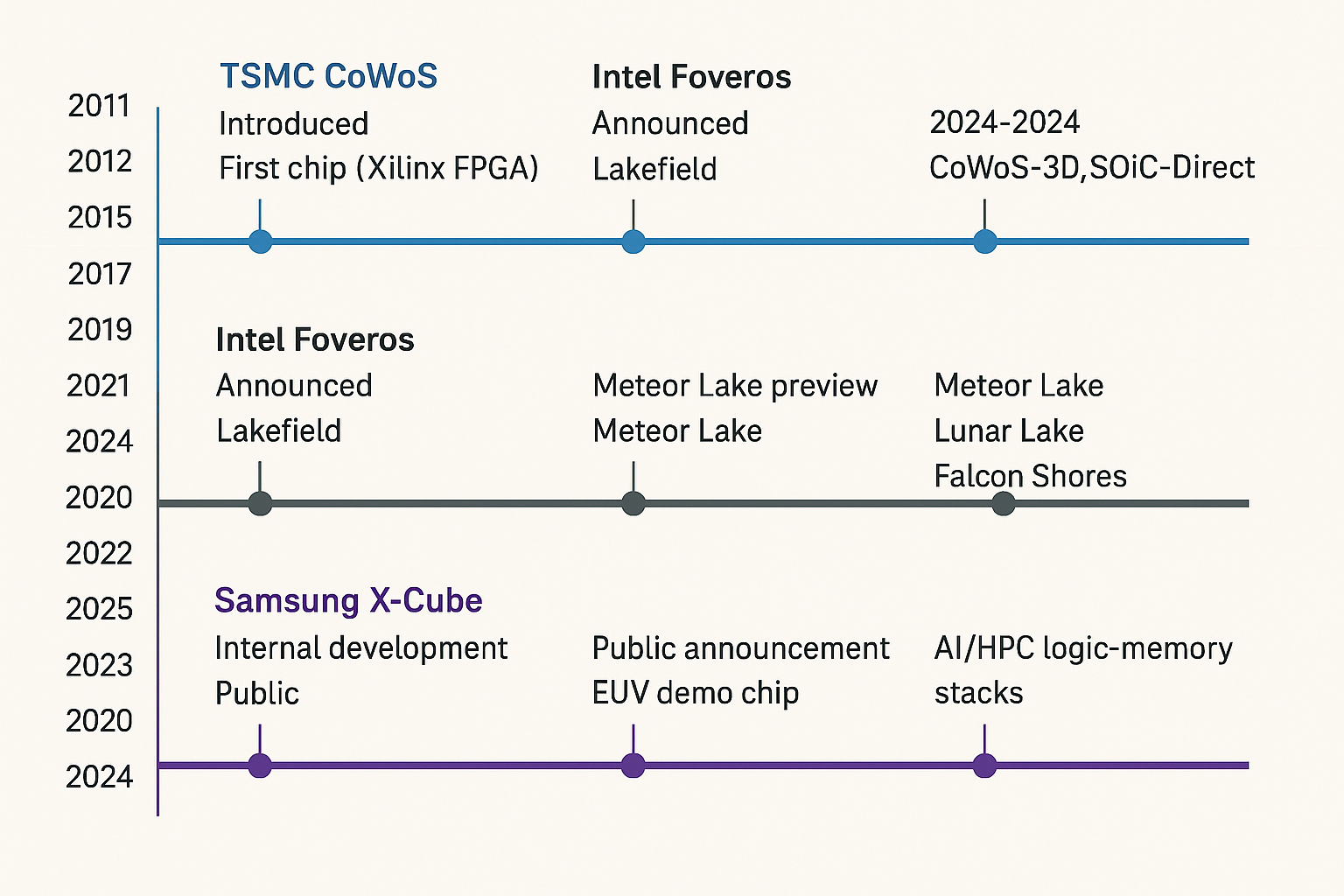
Timeline
TSMC CoWoS
├─ 2011: Introduced
├─ 2012: First chip (Xilinx FPGA)
├─ 2015: NVIDIA Pascal
├─ 2017: CoWoS-S
├─ 2020: SoIC (3D complement)
├─ 2022: CoWoS-R
└─ 2024–25: CoWoS-3D, SoIC-Direct
Intel Foveros
├─ 2018: Announced
├─ 2019: Lakefield
├─ 2022: Meteor Lake preview
├─ 2024: Meteor Lake launch
└─ 2025: Lunar Lake, Falcon Shores
Samsung X-Cube
├─ 2019: Internal development
├─ 2020: Public announcement
├─ 2021: EUV demo chip
├─ 2023: Pilot HBM3 stacking
└─ 2025: AI/HPC logic-memory stacks

Conclusion
-
TSMC CoWoS is the industry’s most mature and widely used 2.5D packaging technology, excelling in bandwidth and chiplet integration. It’s evolving toward 3D with CoWoS-R and SoIC.
-
Intel Foveros represents the most advanced logic-on-logic 3D integration, enabling chiplet-based CPUs with flexible node partitioning. However, it’s more thermally and yield constrained.
-
Samsung X-Cube is still developing but shows promise in tight TSV pitch, signal integrity, and logic-memory vertical integration, especially if paired with Samsung’s HBM and foundry ecosystems.


Captain America: Can Elon Musk Save America’s Chip Manufacturing Industry?